Superconducting NbN Resonator Parametric Amplifiers for Millimetre Wavelengths
Publication
Metrics
Paper Preview
Abstract
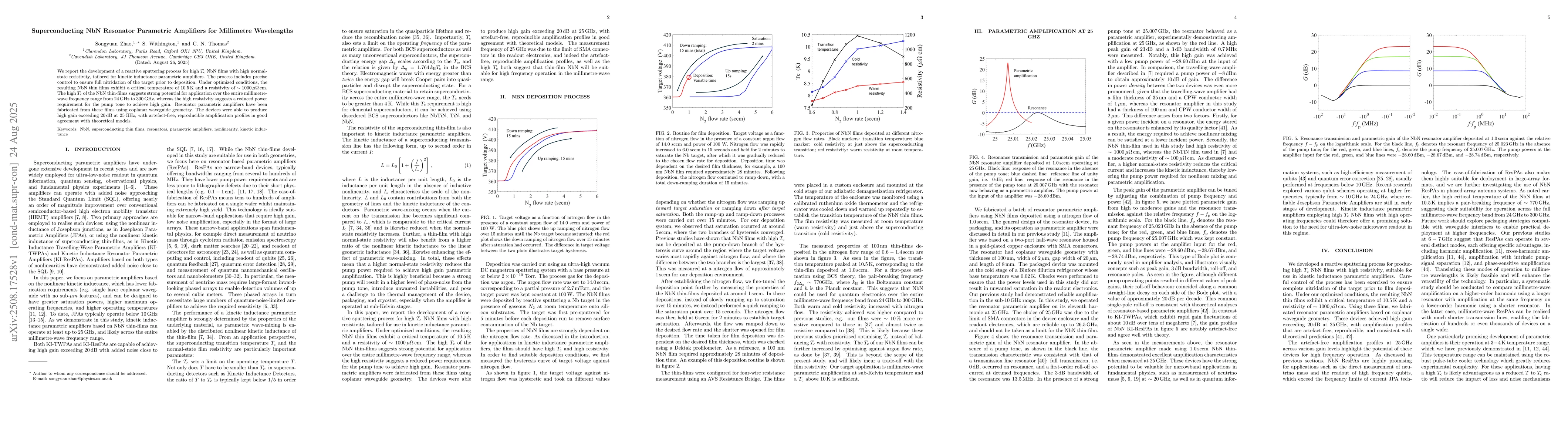
We report the development of a reactive sputtering process for high $T_\mathrm{c}$ NbN films with high normal-state resistivity, tailored for kinetic inductance parametric amplifiers. The process includes precise control to ensure full nitridation of the target prior to deposition. Under optimized conditions, the resulting NbN thin films exhibit a critical temperature of $10.5\,\mathrm{K}$ and a resistivity of $\sim1000\,\mathrm{\mu\Omega\,cm}$. The high $T_\mathrm{c}$ of the NbN thin-films suggests strong potential for application over the entire millimetre-wave frequency range from $24\,\mathrm{GHz}$ to $300\,\mathrm{GHz}$, whereas the high resistivity suggests a reduced power requirement for the pump tone to achieve high gain. Resonator parametric amplifiers have been fabricated from these films using coplanar waveguide geometry. The devices were able to produce high gain exceeding $20\,\mathrm{dB}$ at $25\,\mathrm{GHz}$, with artefact-free, reproducible amplification profiles in good agreement with theoretical models.
AI Key Findings
Get AI-generated insights about this paper's methodology, results, significance, and more — seven facets brought into focus.
Discussion 0