Superconductor Electronics Fabrication Process with MoN$_x$ Kinetic Inductors and Self-Shunted Josephson Junctions
Publication
Metrics
AI Quick Summary
This research develops a fabrication process for advanced superconductor electronics using self-shunted Josephson junctions and thin-film MoN$_x$ kinetic inductors to enhance integration scale. Mo$_2$N films show adjustable inductance and suitable superconducting properties, while self-shunted JJs with Si$_{1-x}$Nb$_x$ barriers exhibit complex electron transport mechanisms and variable Josephson characteristics.
Paper Preview
Abstract
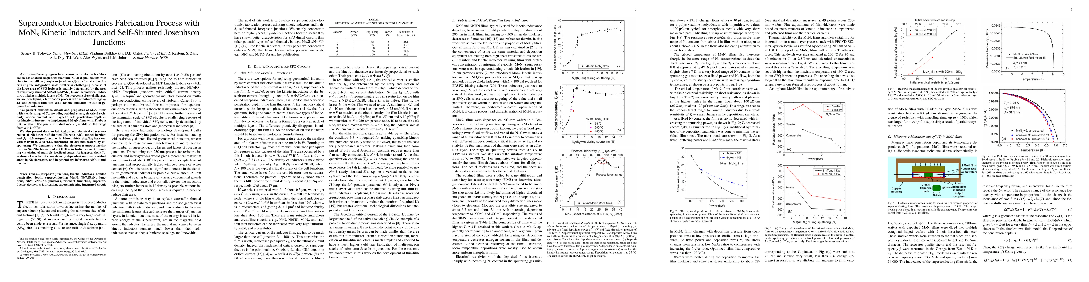
Recent progress in superconductor electronics fabrication has enabled single-flux-quantum (SFQ) digital circuits with close to one million Josephson junctions (JJs) on 1-cm$^2$ chips. Increasing the integration scale further is challenging because of the large area of SFQ logic cells, mainly determined by the area of resistively shunted Nb/AlO$_x$-Al/Nb JJs and geometrical inductors utilizing multiple layers of Nb. To overcome these challenges, we are developing a fabrication process with self-shunted high-J$_c$ JJs and compact thin-film MoN$_x$ kinetic inductors instead of geometrical inductors. We present fabrication details and properties of MoN$_x$ films with a wide range of T$_c$, including residual stress, electrical resistivity, critical current, and magnetic field penetration depth {\lambda}$_0$. As kinetic inductors, we implemented Mo$_2$N films with T$_c$ about 8 K, {\lambda}$_0$ about 0.51 {\mu}m, and inductance adjustable in the range from 2 to 8 pH/sq. We also present data on fabrication and electrical characterization of Nb-based self-shunted JJs with AlO$_x$ tunnel barriers and J$_c$ = 0.6 mA/{\mu}m$^2$, and with 10-nm thick Si$_{1-x}$Nb$_x$ barriers, with x from 0.03 to 0.15, fabricated on 200-mm wafers by co-sputtering. We demonstrate that the electron transport mechanism in Si$_{1-x}$Nb$_x$ barriers at x < 0.08 is inelastic resonant tunneling via chains of multiple localized states. At larger x, their Josephson characteristics are strongly dependent on x and residual stress in Nb electrodes, and in general are inferior to AlO$_x$ tunnel barriers.
AI Key Findings
Get AI-generated insights about this paper's methodology, results, significance, and more — seven facets brought into focus.
Impact
Paper Details
PDF Preview
Key Terms
Citation Network
Current paper (gray), citations (green), references (blue)
Display is limited for performance on very large graphs.
Discussion 0