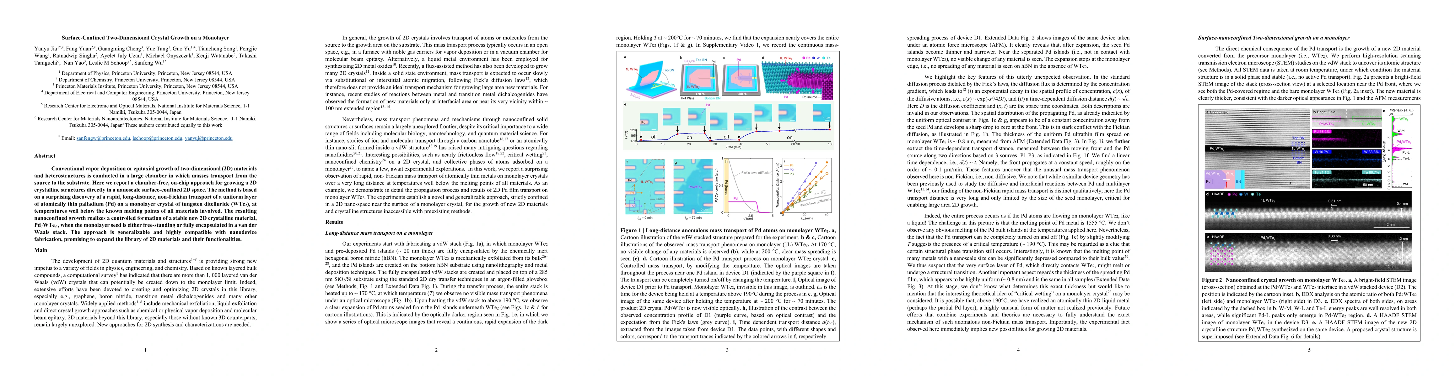
Publication
Metrics
AI Quick Summary
This paper presents a novel chamber-free, on-chip method for growing two-dimensional (2D) crystalline structures in a confined nanoscale space, achieving rapid, non-Fickian transport of palladium on a tungsten ditelluride monolayer at low temperatures. The technique enables the formation of a stable new 2D material, Pd7WTe2, and is highly compatible with nanodevice fabrication.
Paper Preview
Abstract
Conventional vapor deposition or epitaxial growth of two-dimensional (2D) materials and heterostructures is conducted in a large chamber in which masses transport from the source to the substrate. Here we report a chamber-free, on-chip approach for growing a 2D crystalline structures directly in a nanoscale surface-confined 2D space. The method is based on a surprising discovery of a rapid, long-distance, non-Fickian transport of a uniform layer of atomically thin palladium (Pd) on a monolayer crystal of tungsten ditelluride (WTe2), at temperatures well below the known melting points of all materials involved. The resulting nanoconfined growth realizes a controlled formation of a stable new 2D crystalline material, Pd7WTe2 , when the monolayer seed is either free-standing or fully encapsulated in a van der Waals stack. The approach is generalizable and highly compatible with nanodevice fabrication, promising to expand the library of 2D materials and their functionalities.
AI Key Findings
Get AI-generated insights about this paper's methodology, results, significance, and more — seven facets brought into focus.
Impact
Paper Details
Authors
PDF Preview
Key Terms
Citation Network
Current paper (gray), citations (green), references (blue)
Display is limited for performance on very large graphs.
Discussion 0