Publication
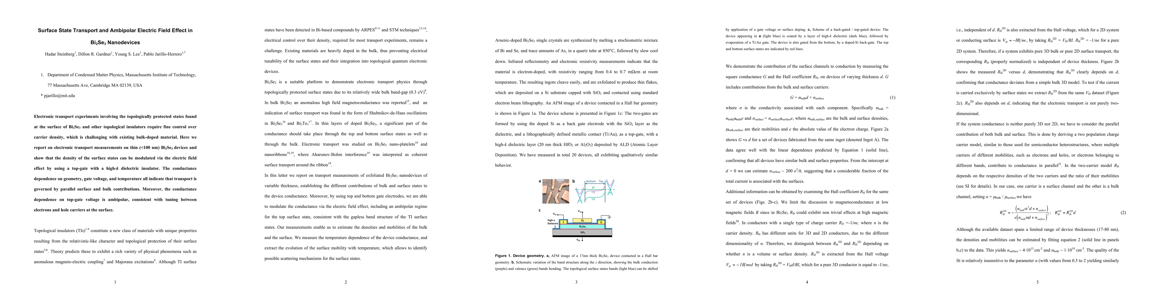
Metrics
AI Quick Summary
This paper investigates electronic transport in thin Bi2Se3 nanodevices, demonstrating that surface state carrier density can be modulated via an electric field effect using a top-gate with a high-k dielectric. The study reveals ambidextrous conductance behavior, indicating control over both electron and hole carriers at the surface.
Paper Preview
Abstract
Electronic transport experiments involving the topologically protected states found at the surface of Bi2Se3 and other topological insulators require fine control over carrier density, which is challenging with existing bulk-doped material. Here we report on electronic transport measurements on thin (<100 nm) Bi2Se3 devices and show that the density of the surface states can be modulated via the electric field effect by using a top-gate with a high-k dielectric insulator. The conductance dependence on geometry, gate voltage, and temperature all indicate that transport is governed by parallel surface and bulk contributions. Moreover, the conductance dependence on top-gate voltage is ambipolar, consistent with tuning between electrons and hole carriers at the surface.
AI Key Findings
Get AI-generated insights about this paper's methodology, results, significance, and more — seven facets brought into focus.
Impact
Paper Details
PDF Preview
Key Terms
Citation Network
Current paper (gray), citations (green), references (blue)
Display is limited for performance on very large graphs.
Discussion 0