Suspension and simple optical characterization of two-dimensional membranes
Publication
Metrics
AI Quick Summary
Researchers developed a simple method to suspend two-dimensional materials like graphene and NbSe2 in an electronic circuit using photoresists and solvents, enabling quick optical characterization of their number of layers and gap separation.
Paper Preview
Abstract
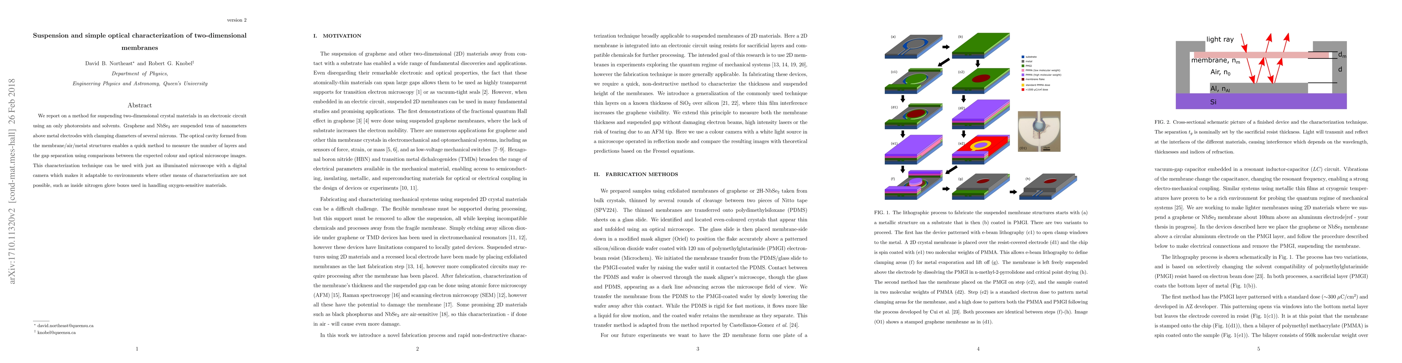
We report on a method for suspending two-dimensional crystal materials in an electronic circuit using an only photoresists and solvents. Graphene and NbSe${}_2$ are suspended tens of nanometers above metal electrodes with clamping diameters of several microns. The optical cavity formed from the membrane/air/metal structures enables a quick method to measure the number of layers and the gap separation using comparisons between the expected colour and optical microscope images. This characterization technique can be used with just an illuminated microscope with a digital camera which makes it adaptable to environments where other means of characterization are not possible, such as inside nitrogen glove boxes used in handling oxygen-sensitive materials.
AI Key Findings
Get AI-generated insights about this paper's methodology, results, significance, and more — seven facets brought into focus.
Impact
Paper Details
PDF Preview
Key Terms
Citation Network
Current paper (gray), citations (green), references (blue)
Display is limited for performance on very large graphs.
Discussion 0