Publication
Metrics
AI Quick Summary
This paper details the fabrication and characterization of multiwall MoS2 nanotube and nanoribbon field-effect transistors, grown via chemical transport. The devices exhibit n-type behavior with high ON/OFF current ratios and responsivity, demonstrating potential for optoelectronic applications.
Paper Preview
Abstract
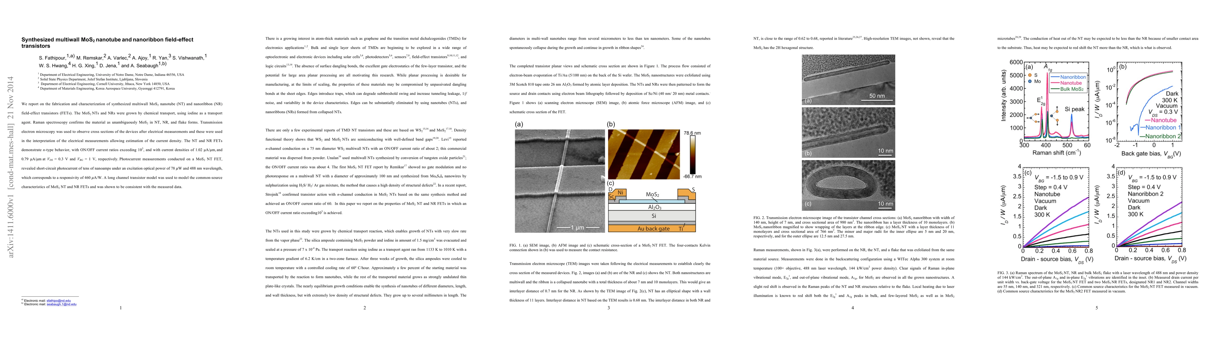
We report on the fabrication and characterization of synthesized multiwall MoS2 nanotube (NT) and nanoribbon (NR) field-effect transistors (FETs). The MoS2 NTs and NRs were grown by chemical transport, using iodine as a transport agent. Raman spectroscopy confirms the material as unambiguously MoS2 in NT, NR, and flake forms. Transmission electron microscopy was used to observe cross sections of the devices after electrical measurements and these were used in the interpretation of the electrical measurements allowing estimation of the current density. The NT and NR FETs demonstrate n-type behavior, with ON/OFF current ratios exceeding 10^3, and with current densities of 1.02 {\mu}A/{\mu}m, and 0.79 {\mu}A/{\mu}m at VDS = 0.3 V and VBG = 1 V, respectively. Photocurrent measurements conducted on a MoS2 NT FET, revealed short-circuit photocurrent of tens of nanoamps under an excitation optical power of 78 {\mu}W and 488 nm wavelength, which corresponds to a responsivity of 460 {\mu}A/W. A long channel transistor model was used to model the common-source characteristics of MoS2 NT and NR FETs and was shown to be consistent with the measured data.
AI Key Findings
Get AI-generated insights about this paper's methodology, results, significance, and more — seven facets brought into focus.
Impact
Paper Details
PDF Preview
Key Terms
Citation Network
Current paper (gray), citations (green), references (blue)
Display is limited for performance on very large graphs.
Discussion 0