Two-photon microscopy combined with automated digital image processing to extract duty cycle, domain uniformity, and period, followed by multivariate regression modeling of poling parameters.
Publication
Metrics
Quick Answers
What methodology did the authors use?
Two-photon microscopy combined with automated digital image processing to extract duty cycle, domain uniformity, and period, followed by multivariate regression modeling of poling parameters. More in Methodology →
What are the key results?
Temperature is the dominant factor controlling duty cycle and domain uniformity, with optimal values around 160 °C. — Multiple voltage pulses and moderate electrode gaps synergistically improve inversion completeness and reduce spatial fluctuations. More in Key Results →
Why is this work significant?
Provides a data‑driven, wafer‑scale framework for optimizing PPLN fabrication, accelerating production of high‑performance lithium‑niobate photonic integrated circuits. More in Significance →
What are the main limitations?
Residual variance remains due to fabrication imperfections and imaging resolution limits. — The statistical model is specific to the studied x‑cut thin‑film geometry and may not generalize without retraining. More in Limitations →
Abstract
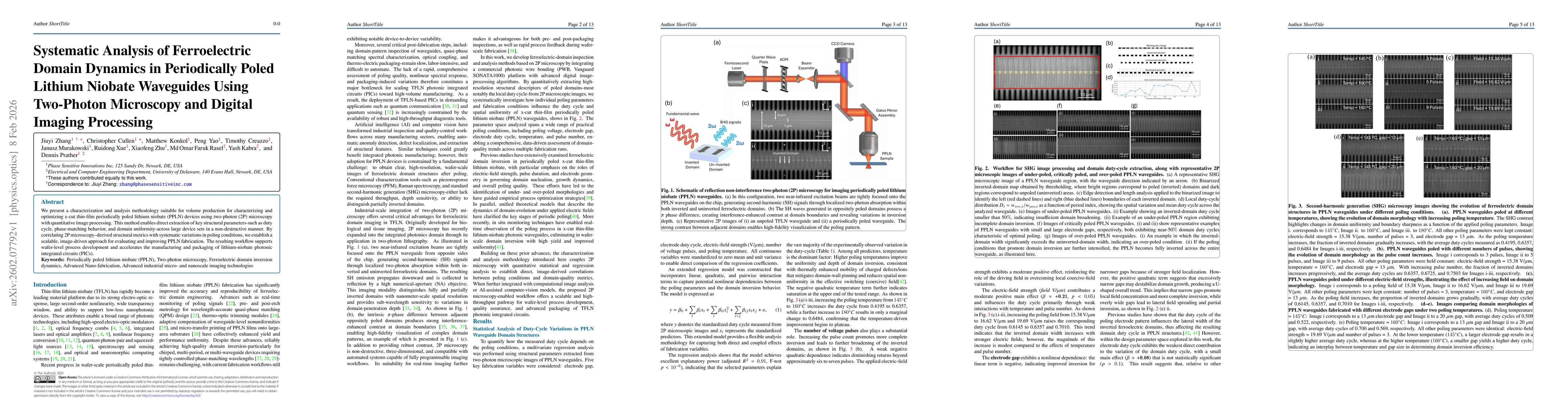
We present a characterization and analysis methodology suitable for volume production for characterizing and optimizing x-cut thin-film periodically poled lithium niobate (PPLN) devices using two-photon (2P) microscopy with quantitative image processing. This method enables direct extraction of key structural parameters, such as duty cycle, phase-matching behavior, and domain uniformity, across large device sets in a non-destructive manner. By correlating 2P microscopy-derived structural metrics with systematic variations in poling conditions, we establish a scalable, image-driven approach for evaluating and improving PPLN fabrication. The resulting workflow supports wafer-level process development and accelerates the manufacturing and packaging of lithium niobate photonic integrated circuits (PICs).
Key Findings, in focus
Seven facets of this paper, analysed and brought into focus by AI.
Provides a data‑driven, wafer‑scale framework for optimizing PPLN fabrication, accelerating production of high‑performance lithium‑niobate photonic integrated circuits.
- Temperature is the dominant factor controlling duty cycle and domain uniformity, with optimal values around 160 °C.
- Multiple voltage pulses and moderate electrode gaps synergistically improve inversion completeness and reduce spatial fluctuations.
- An extended regression model predicts a practical poling window (≈160 °C, 5–7 pulses, 15 V/µm, 14–17 µm gap) that yields high-duty-cycle, uniform PPLN waveguides.
Provides a data‑driven, wafer‑scale framework for optimizing PPLN fabrication, accelerating production of high‑performance lithium‑niobate photonic integrated circuits.
An image‑driven regression framework that quantitatively links poling parameters to duty cycle and domain uniformity, including interaction terms and validated residual diagnostics.
First large‑scale, systematic statistical analysis of ferroelectric domain dynamics in PPLN waveguides using two‑photon microscopy, enabling wafer‑level process optimization.
- Residual variance remains due to fabrication imperfections and imaging resolution limits.
- The statistical model is specific to the studied x‑cut thin‑film geometry and may not generalize without retraining.
- Integrate machine‑learning surrogates and Bayesian optimization to search optimal poling conditions across device variants.
- Develop AI models that predict nonlinear conversion efficiency directly from 2P images, eliminating the need for separate optical measurements.
Discussion 0