The study combines atomistic tight-binding non-equilibrium Green's-function calculations to model coherent transport across CNT junctions (single SWCNT–SWCNT, double-walled, and triple-walled configurations) and analyzes the effects of perpendicular magnetic fields. It employs analytically solvable minimal models to identify transport regimes and interprets results using an electron-waveguide framework to connect microscopic interference mechanisms to design principles for high-conductance CNT conductors.
Taming quantum interference: a route to high electrical conductance in carbon nanotube assemblies
Publication
Metrics
AI Quick Summary
The paper shows that electron interference at carbon nanotube junctions largely controls electrical conductance, and that junction architecture (single, double, or triple-walled CNTs) shapes transmission in predictable ways. Using atomistic calculations and simple models, it demonstrates how overlap, doping, magnetic fields, and added pathways create high-conductance windows or filtering effects, offering design rules for stable, high-conductance CNT conductors.
Quick Answers
What is "Taming quantum interference: a route to high electrical conductance in carbon nanotube assemblies" about?
The paper shows that electron interference at carbon nanotube junctions largely controls electrical conductance, and that junction architecture (single, double, or triple-walled CNTs) shapes transmission in predictable ways. Using atomistic calculations and simple models, it demonstrates how overlap, doping, magnetic fields, and added pathways create high-conductance windows or filtering effects, offering design rules for stable, high-conductance CNT conductors.
What methodology did the authors use?
The study combines atomistic tight-binding non-equilibrium Green's-function calculations to model coherent transport across CNT junctions (single SWCNT–SWCNT, double-walled, and triple-walled configurations) and analyzes the effects of perpendicular magnetic fields. It employs analytically solvable minimal models to identify transport regimes and interprets results using an electron-waveguide framework to connect microscopic interference mechanisms to design principles for high-conductance CNT conductors. More in Methodology →
What are the key results?
High-transmission windows in single SWCNT–SWCNT junctions are governed primarily by overlap length, doping, and magnetic field, with gateway states enhancing conductance when some CNT subbands are gapped. — Magnetic fields can restore transmission by lifting interference blockade in certain configurations, illustrating field-tunable interference control at junctions. More in Key Results →
Why is this work significant?
The work translates microscopic quantum interference mechanisms at CNT junctions into practical design principles for achieving high-conductance, field-stable CNT conductors, providing a coherent explanation for observed differences between SWCNT and MWCNT transport in high-field regimes and guiding junction engineering for nanoscale electronics. More in Significance →
What are the main limitations?
The analysis relies on idealized junction geometries and tight-binding models which may not capture all disorder and environmental effects present in real networks. — Perpendicular magnetic-field studies are extensive, but the model may not fully account for temperature-dependent decoherence or phonon interactions at elevated temperatures. More in Limitations →
Abstract
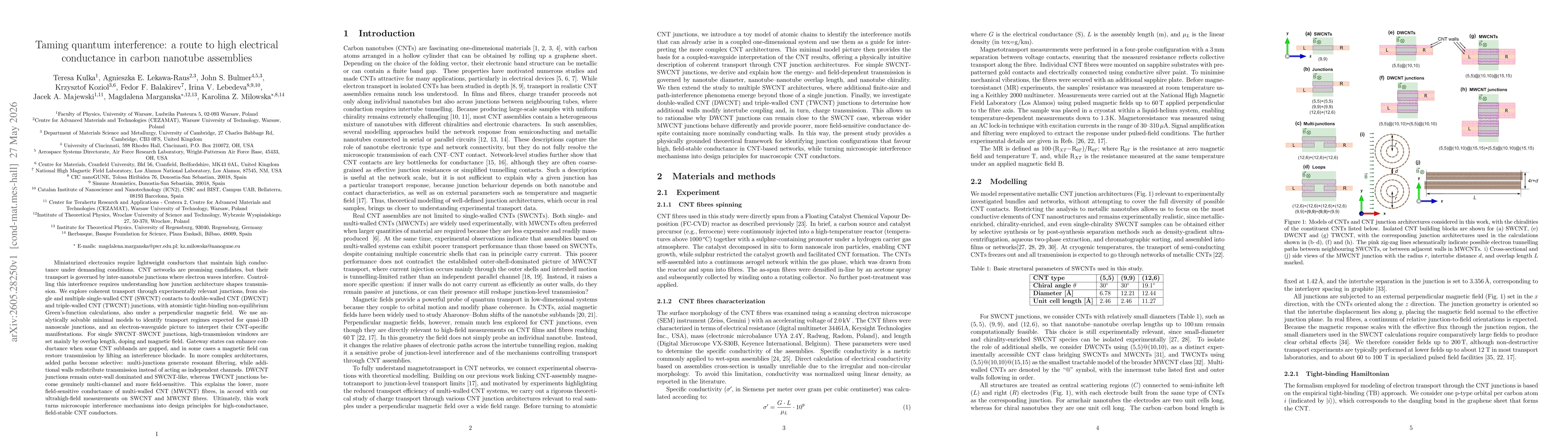
Miniaturized electronics require lightweight conductors that maintain high conductance under demanding conditions. CNT networks are promising candidates, but their transport is governed by inter-nanotube junctions where electron waves interfere. Controlling this interference requires understanding how junction architecture shapes transmission. We explore coherent transport through experimentally relevant junctions, from single and multiple single-walled CNT (SWCNT) contacts to double-walled CNT (DWCNT) and triple-walled CNT (TWCNT) junctions, with atomistic tight-binding non-equilibrium Green's-function calculations, also under a perpendicular magnetic field. We use analytically solvable minimal models to identify transport regimes expected for quasi-1D nanoscale junctions, and an electron-waveguide picture to interpret their CNT-specific manifestations. For single SWCNT--SWCNT junctions, high-transmission windows are set mainly by overlap length, doping and magnetic field. Gateway states can enhance conductance when some CNT subbands are gapped, and in some cases a magnetic field can restore transmission by lifting an interference blockade. In more complex architectures, added paths become selective: multi-junctions generate resonant filtering, while additional walls redistribute transmission instead of acting as independent channels. DWCNT junctions remain outer-wall dominated and SWCNT-like, whereas TWCNT junctions become genuinely multi-channel and more field-sensitive. This explains the lower, more field-sensitive conductance of multi-walled CNT (MWCNT) fibres, in accord with our ultrahigh-field measurements on SWCNT and MWCNT fibres. Ultimately, this work turns microscopic interference mechanisms into design principles for high-conductance, field-stable CNT conductors.
Key Findings, in focus
Seven facets of this paper, analysed and brought into focus by AI.
The work translates microscopic quantum interference mechanisms at CNT junctions into practical design principles for achieving high-conductance, field-stable CNT conductors, providing a coherent explanation for observed differences between SWCNT and MWCNT transport in high-field regimes and guiding junction engineering for nanoscale electronics.
- High-transmission windows in single SWCNT–SWCNT junctions are governed primarily by overlap length, doping, and magnetic field, with gateway states enhancing conductance when some CNT subbands are gapped.
- Magnetic fields can restore transmission by lifting interference blockade in certain configurations, illustrating field-tunable interference control at junctions.
- In multi-junction architectures, added paths lead to resonant filtering while outer-wall dominance persists in DWCNT junctions, and TWCNT junctions become genuinely multi-channel and more field-sensitive.
- MWCNT fibres exhibit lower and more field-sensitive conductance consistent with experimental ultrahigh-field measurements, due to redistribution of transmission among channels rather than simple parallel-channel behavior.
The work translates microscopic quantum interference mechanisms at CNT junctions into practical design principles for achieving high-conductance, field-stable CNT conductors, providing a coherent explanation for observed differences between SWCNT and MWCNT transport in high-field regimes and guiding junction engineering for nanoscale electronics.
A rigorous atomistic-transport framework (tight-binding NEGF) complemented by analytically tractable models, enabling interpretation of junction-level interference and providing design rules for achieving high conductance under strong magnetic fields in CNT assemblies.
First comprehensive junction-level study showing how perpendicular magnetic fields and multi-wall architectures co-determine coherent transport in CNT junctions, linking microscopic interference to macroscopic conductance trends in SWCNT, DWCNT, and TWCNT systems.
- The analysis relies on idealized junction geometries and tight-binding models which may not capture all disorder and environmental effects present in real networks.
- Perpendicular magnetic-field studies are extensive, but the model may not fully account for temperature-dependent decoherence or phonon interactions at elevated temperatures.
- Extend simulations to include disorder, chirality distributions, and thermal fluctuations to assess robustness of the design principles in realistic CNT assemblies.
- Experimentally validate predicted field-tunability across a broader range of junction architectures, including mixed-chirality networks.
- Explore optimization strategies for overlap length and gateway-state engineering to maximize field-stable high conductance in scalable CNT films and fibres.
Discussion 0