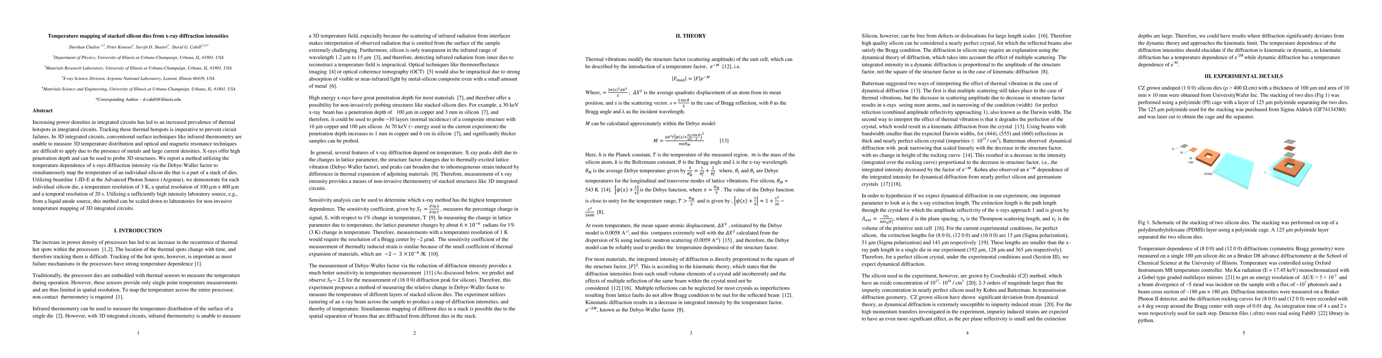
Temperature mapping of stacked silicon dies from x-ray diffraction intensities
Publication
Metrics
AI Quick Summary
This paper presents a novel method for non-invasive temperature mapping of stacked silicon dies in 3D integrated circuits using x-ray diffraction intensities. The technique leverages the temperature dependence of x-ray diffraction via the Debye-Waller factor, achieving a temperature resolution of 3 K and spatial resolution of 100 um x 400 um with a temporal resolution of 20 s.
Paper Preview
Abstract
Increasing power densities in integrated circuits has led to an increased prevalence of thermal hotspots in integrated circuits. Tracking these thermal hotspots is imperative to prevent circuit failures. In 3D integrated circuits, conventional surface techniques like infrared thermometry are unable to measure 3D temperature distribution and optical and magnetic resonance techniques are difficult to apply due to the presence of metals and large current densities. X-rays offer high penetration depth and can be used to probe 3D structures. We report a method utilizing the temperature dependence of x-rays diffraction intensity via the Debye-Waller factor to simultaneously map the temperature of an individual silicon die that is a part of a stack of dies. Utilizing beamline 1-ID-E at the Advanced Photon Source (Argonne), we demonstrate for each individual silicon die, a temperature resolution of 3 K, a spatial resolution of 100 um x 400 um and a temporal resolution of 20 s. Utilizing a sufficiently high intensity laboratory source, e.g., from a liquid anode source, this method can be scaled down to laboratories for non-invasive temperature mapping of 3D integrated circuits.
AI Key Findings
Get AI-generated insights about this paper's methodology, results, significance, and more — seven facets brought into focus.
Impact
Paper Details
Authors
PDF Preview
Key Terms
Citation Network
Current paper (gray), citations (green), references (blue)
Display is limited for performance on very large graphs.
Discussion 0