ArxivLens

Quick Summary:

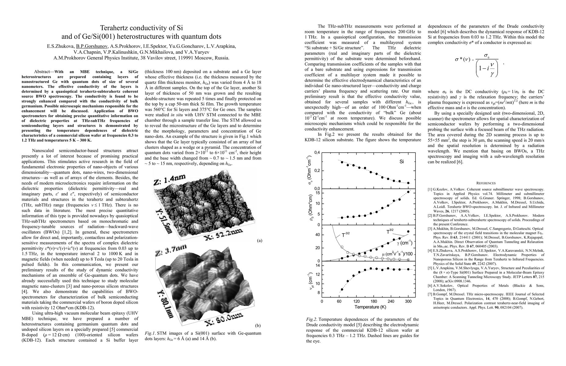
This research investigates the terahertz conductivity of Si and Ge/Si(001) heterostructures with quantum dots, revealing a significant enhancement using MBE and BWO spectroscopy. The study discusses possible microscopic mechanisms for this enhancement and demonstrates the utility of BWO spectrometers for precise dielectric property measurements in semiconductors at THz frequencies.

Journal Reference: 33rd International Conference on Infrared, Millimeter and Terahertz Waves, 2008. IRMMW-THz 2008. 15-19 Sept. 2008, Pasadena, CA, p. 1-2
DOI: 10.1109/ICIMW.2008.4665871
arXiv Id: 1003.3136
Comments: Proc. 33rd International Conference on Infrared, Millimeter, and Terahertz Waves (IRMMW-THz 2008), September 15-19, 2008, California Institute of Technology, Pasadena, California, USA.
Date Published: 2011-05-17
Date Updated: 2011-05-17

Key Terms (TF-IDF):

conductivity (0.315)
thz (0.298)
layers (0.275)
dielectric (0.263)
ge (0.248)
frequencies (0.232)
commercial (0.172)
prepared (0.167)
dots (0.161)
silicon (0.157)
obtaining (0.156)
si (0.156)
microscopic (0.145)
responsible (0.141)
enhancement (0.140)
coherent (0.135)
spectroscopy (0.132)
containing (0.132)
precise (0.131)
enhanced (0.130)
License: http://arxiv.org/licenses/nonexclusive-distrib/1.0/

Summary:

With an MBE technique, a Si/Ge heterostructures are prepared containing layers of nanostructured Ge with quantum dots of size of several nanometers. The effective conductivity of the layers is determined by a quasioptical terahertz-subterahertz coherent source BWO spectroscopy. The conductivity is found to be strongly enhanced compared with the conductivity of bulk germanium. Possible microscopic mechanisms responsible for the enhancement will be discussed. Application of BWO spectrometers for obtaining precise quantitative information on of dielectric properties at THz-subTHz frequencies of semiconducting layers and structures is demonstrated by presenting the temperature dependences of dielectric characteristics of a commercial silicon wafer at frequencies 0.3 to 1.2 THz and temperatures 5K-300K.

Citation & Reference Network Visualization

This graph shows how this paper is connected to other research. The current paper is shown in dark gray, papers that cite it are in green, and papers it references are in blue. You can:

Current Paper
Papers citing this work (Citations)
Papers cited by this work (References)

• Hover over any node to see the paper title

• Click a node to view that paper's details

• Drag nodes to rearrange the graph

• Use the zoom controls (bottom right) to zoom in/out

Citations and References

No citations found for this paper.

Comments (0)

This website uses cookies to ensure you get the best experience. Learn more