01
MethodologyHow they did it
Brief description of the research methodology used
This paper investigates the dissociation of (a+c) misfit dislocations at the InGaN/GaN interface, revealing that they split into two Frank-Shockley partial dislocations. Atomistic simulations show a 3/5 atom ring structure in the core of the partial dislocations, suggesting the separation is likely due to climb induced by mismatch stress.
This paper investigates the dissociation of (a+c) misfit dislocations at the InGaN/GaN interface, revealing that they split into two Frank-Shockley partial dislocations. Atomistic simulations show a 3/5 atom ring structure in the core of the partial dislocations, suggesting the separation is likely due to climb induced by mismatch stress.
Brief description of the research methodology used More in Methodology →
Main finding 1 — Main finding 2 More in Key Results →
Why this research is important and its potential impact More in Significance →
Limitation 1 — Limitation 2 More in Limitations →
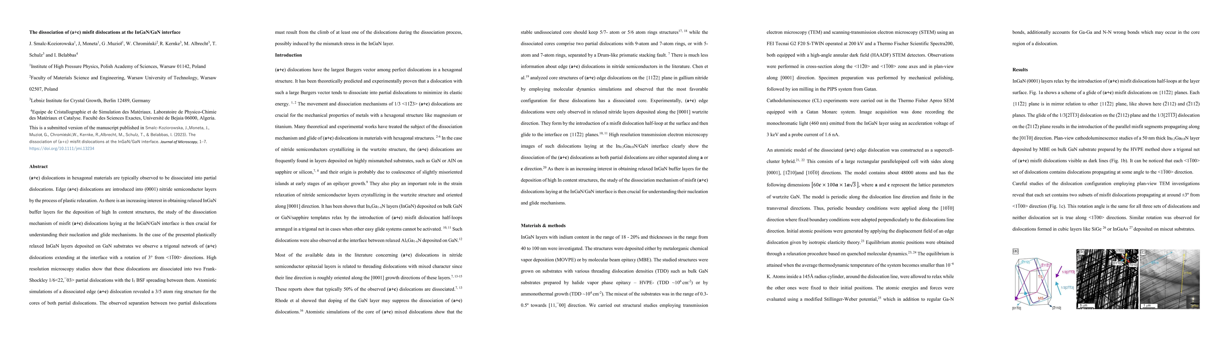
(a+c) dislocations in hexagonal materials are typically observed to be dissociated into partial dislocations. Edge (a+c) dislocations are introduced into (0001) nitride semiconductor layers by the process of plastic relaxation. As there is an increasing interest in obtaining relaxed InGaN buffer layers for the deposition of high In content structures, the study of the dissociation mechanism of misfit (a+c) dislocations laying at the InGaN/GaN interface is then crucial for understanding their nucleation and glide mechanisms. In the case of the presented plastically relaxed InGaN layers deposited on GaN substrates we observe a trigonal network of (a+c) dislocations extending at the interface with a rotation of 3 degrees from <1-100> directions. High resolution microscopy studies show that these dislocations are dissociated into two Frank-Shockley 1/6<2-203> partial dislocations with the I1 BSF spreading between them. Atomistic simulations of a dissociated edge (a+c) dislocation revealed a 3/5 atom ring structure for the cores of both partial dislocations. The observed separation between two partial dislocations must result from the climb of at least one of the dislocations during the dissociation process, possibly induced by the mismatch stress in the InGaN layer.
Seven facets of this paper, analysed and brought into focus by AI.
Why this research is important and its potential impact
Brief description of the research methodology used
Why this research is important and its potential impact
Main technical or theoretical contribution
What makes this work novel or different from existing research
Current paper (gray), citations (green), references (blue)
Display is limited for performance on very large graphs.
Discussion 0