The Effect of Different Wavelengths on Porous Silicon Formation Process
Publication
Metrics
AI Quick Summary
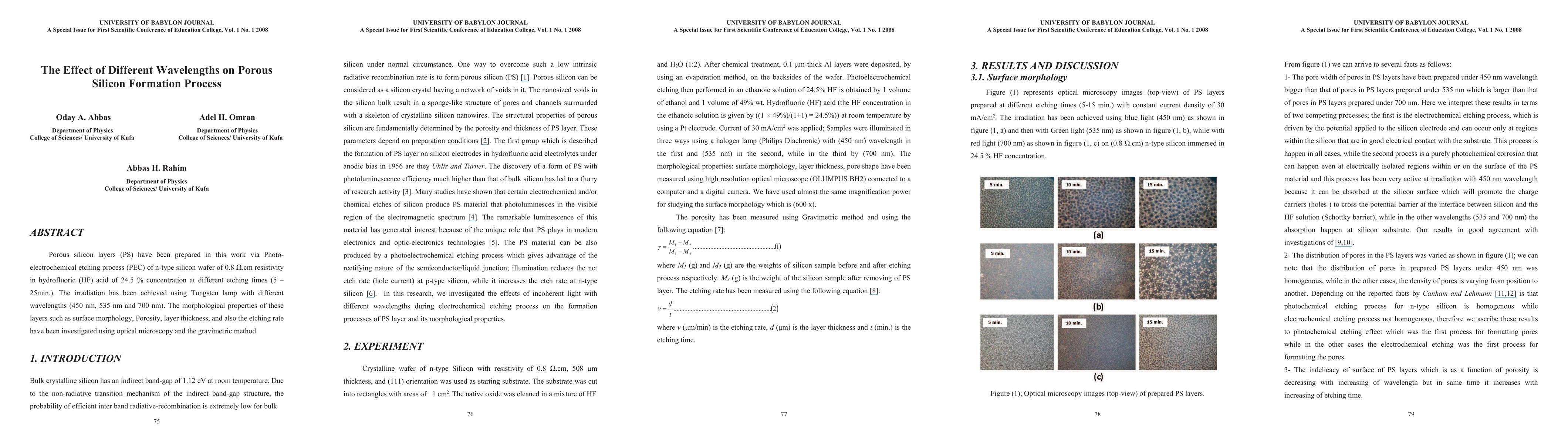
This study investigates the impact of various wavelengths (450 nm, 535 nm, and 700 nm) on the formation of porous silicon layers via photoelectrochemical etching, examining surface morphology, porosity, and etching rates using optical microscopy and gravimetric methods. Different etching times were applied to n-type silicon wafers in 24.5% hydrofluoric acid.
Paper Preview
Abstract
Porous silicon layers (PS) have been prepared in this work via Photoelectrochemical etching process (PEC) of n type silicon wafer of 0.8 ohm.cm resistivity in hydrofluoric (HF) acid of 24.5 precent concentration at different etching times (5 to 25 min.). The irradiation has been achieved using Tungsten lamp with different wavelengths (450 nm, 535 nm and 700 nm). The morphological properties of these layers such as surface morphology, Porosity, layer thickness, and also the etching rate have been investigated using optical microscopy and the gravimetric method.
AI Key Findings
Get AI-generated insights about this paper's methodology, results, significance, and more — seven facets brought into focus.
Impact
Paper Details
PDF Preview
Key Terms
Citation Network
Current paper (gray), citations (green), references (blue)
Display is limited for performance on very large graphs.
Discussion 0