Summary
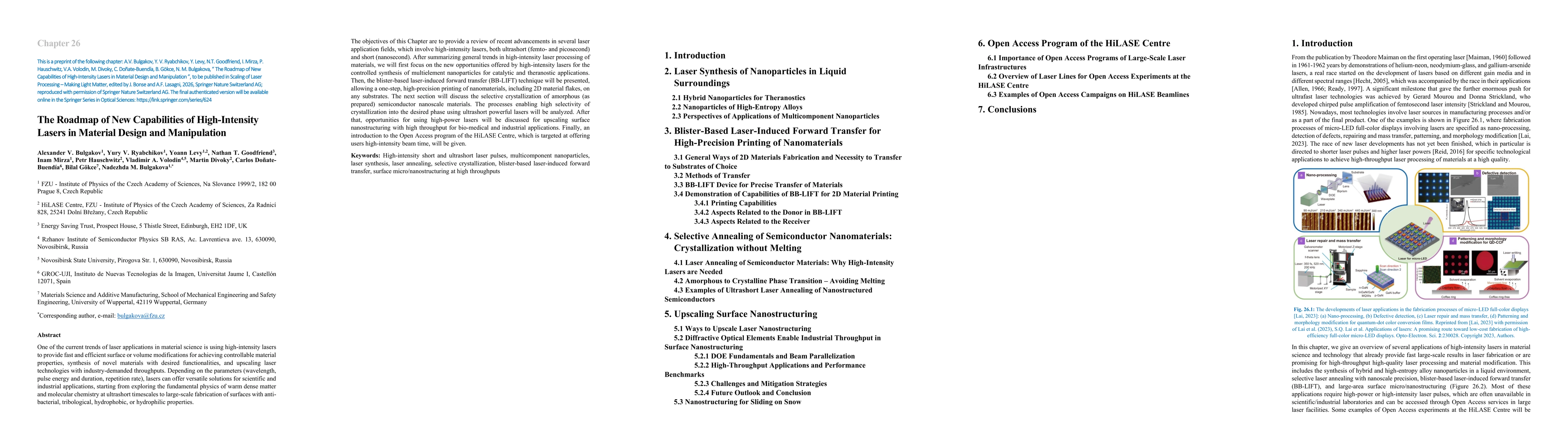
One of the current trends of laser applications in material science is using high-intensity lasers to provide fast and efficient surface or volume modifications for achieving controllable material properties, synthesis of novel materials with desired functionalities, and upscaling laser technologies with industry-demanded throughputs. Depending on the parameters, lasers can offer versatile solutions for scientific and industrial applications, starting from exploring the fundamental physics of warm dense matter and molecular chemistry at ultrashort timescales to large-scale fabrication of surfaces with anti-bacterial, tribological, hydrophobic, or hydrophilic properties. The objectives of this Chapter are to provide a review of recent advancements in several laser application fields, which involve high-intensity lasers, both ultrashort (femto- and picosecond) and short (nanosecond). After summarizing general trends in high-intensity laser processing of materials, we will first focus on the new opportunities offered by high-intensity lasers for the controlled synthesis of multielement nanoparticles for catalytic and theranostic applications. Then, the blister-based laser-induced forward transfer (BB-LIFT) technique will be presented, allowing a one-step, high-precision printing of nanomaterials on any substrates. The next section will discuss the selective crystallization of amorphous (as prepared) semiconductor nanoscale materials. The processes enabling high selectivity of crystallization into the desired phase using ultrashort powerful lasers will be analyzed. After that, opportunities for using high-power lasers will be discussed for upscaling surface nanostructuring with high throughput for bio-medical and industrial applications. Finally, an introduction to the Open Access program of the HiLASE Centre, which is targeted at offering users high-intensity beam time, will be given.
AI Key Findings
Generated Sep 29, 2025
Methodology
The research employs advanced laser processing techniques, including ultrafast laser ablation, diffractive optical elements (DOEs) for beam splitting, and high-speed scanning systems to achieve large-area nanostructuring. It integrates computational modeling and experimental validation to optimize parameters for surface texturing and pattern formation.
Key Results
- Achieved high-throughput surface nanostructuring with sub-micrometer resolution using DOE-based multi-beam systems.
- Demonstrated significant improvements in processing speed, reaching up to 1300 cm²/min for LIPSS generation.
- Enabled complex 3D microstructures and functional surface patterns for biomedical and industrial applications.
Significance
This research advances industrial manufacturing by enabling rapid, precise, and scalable surface texturing for applications in biomedical devices, tribology, photonics, and energy-harvesting systems, potentially reducing costs and improving performance.
Technical Contribution
The work introduces a novel approach to industrial-scale nanostructuring using diffractive optical elements for parallel beam splitting, enabling high-speed, large-area fabrication with sub-micrometer precision.
Novelty
This research stands out by combining advanced DOE technology with high-speed scanning and multi-beam processing to achieve unprecedented throughput and resolution in surface nanostructuring, surpassing traditional methods like EBL and mechanical texturing.
Limitations
- DOE-based systems face challenges in maintaining uniformity and diffraction efficiency at very high sub-beam counts.
- Thermal management and beam alignment complexities increase with higher power and multi-beam configurations.
Future Work
- Development of adaptive DOE systems for real-time optimization of beam distribution and intensity.
- Integration of machine learning for predictive modeling of nanostructuring outcomes.
- Exploration of hybrid approaches combining DOEs with other high-throughput techniques like DLIP and polygon scanning.
Comments (0)