Summary
Solid-melt interfaces play a pivotal role in governing crystal growth and metal-mediated epitaxy of gallium nitride (GaN) and other semiconductor materials. Using atomistic simulations based on machine-learning interatomic potentials (MLIPs), we uncover that multiple layers of Ga atoms at the GaN-Ga melt interface form structurally ordered and electronically charged configurations that are critical for the growth kinetics of GaN. These ordered layers modulate the free energy landscape (FEL) for N adsorption and substantially reduce the migration barriers for N at the interface compared to a clean GaN surface. Leveraging these interfacial energetics, kinetic Monte Carlo (KMC) simulations reveal that GaN growth follows a diffusion-controlled, layer-by-layer mechanism, with the FEL for N adsorption emerging as the rate-limiting factor. By incorporating facet-specific FELs and the diffusivity/solubility of N in Ga melt, we develop a predictive, fitting-free transport model that estimates facet-dependent growth rates in the range of ~0.01 to 0.04 nm/s, in agreement with experimental growth rates observed in GaN nanoparticles synthesized by Ga-mediated molecular beam epitaxy (MBE). This multiscale framework offers a generalizable and quantitative approach to link atomic-scale ordering and interfacial energetics to macroscopic phenomena, providing actionable insights for the rational design of metal-mediated epitaxial processes.
AI Key Findings
Generated Sep 30, 2025
Methodology
The study employed molecular dynamics simulations and well-tempered metadynamics to analyze the role of solid-melt interfaces in III-V semiconductor growth. Free-energy calculations were used to quantify migration barriers and diffusivity of nitrogen atoms in liquid gallium.
Key Results
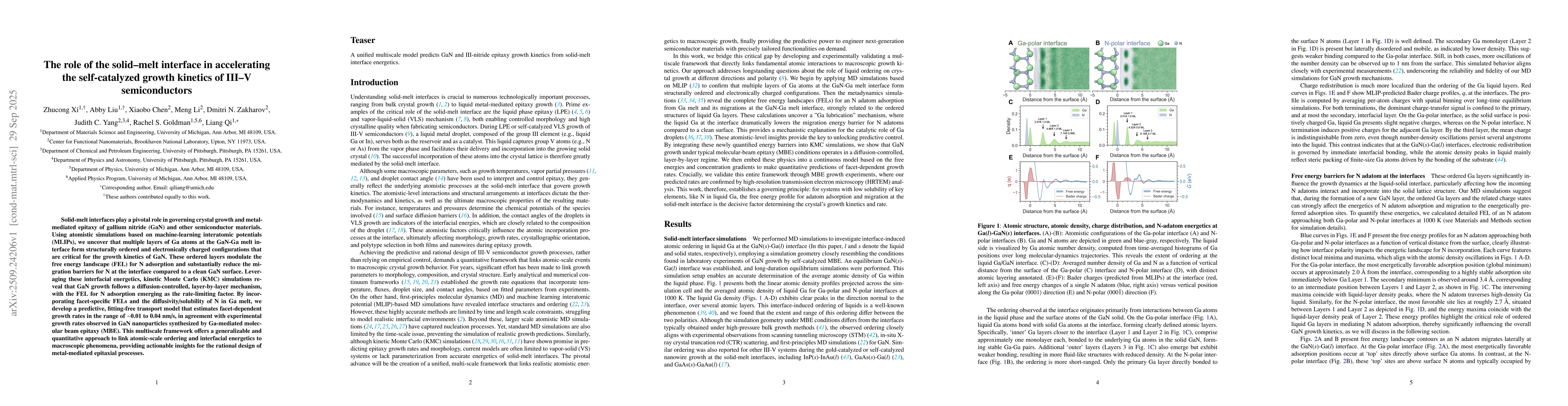
- Migration barriers on clean GaN surfaces are significantly higher (~1.1 eV) compared to liquid-covered interfaces (~0.56 eV).
- Nitrogen solubility in liquid gallium is extremely low, with a calculated solubility limit of ~0.85 eV per atom at 1000 K.
- The bond-counting model shows that N-N bonding at interfaces provides a driving force for nitrogen migration, with a calculated activation energy of ~1.6-1.7 eV.
Significance
This research provides fundamental insights into how solid-melt interfaces accelerate self-catalyzed growth of III-V semiconductors, which is critical for optimizing semiconductor fabrication processes and understanding crystal growth mechanisms.
Technical Contribution
The study introduces a bond-counting model to quantify how N-N bonding at solid-melt interfaces influences migration kinetics, providing a new framework for understanding interface-driven growth mechanisms.
Novelty
This work uniquely combines free-energy calculations with bond-counting analysis to demonstrate how solid-melt interfaces significantly reduce migration barriers, offering a novel perspective on catalytic growth mechanisms in III-V semiconductors.
Limitations
- The simulations are based on idealized models and may not fully capture complex real-world growth conditions.
- The study focuses on GaN systems, limiting generalizability to other III-V materials.
Future Work
- Experimental validation of predicted solubility and migration barriers in liquid gallium.
- Investigation of interface dynamics under varying pressure and temperature conditions.
- Extension of the bond-counting model to other III-V semiconductor systems.
Comments (0)