This paper presents a theoretical model for electrical spin-detection at ferromagnet/semiconductor interfaces, demonstrating that sensitivity strongly depends on bias and is influenced by both microscopic interface properties and macroscopic spin transport in the semiconductor. Numerical results suggest a method for enhancing sensitivity through voltage signal tuning.
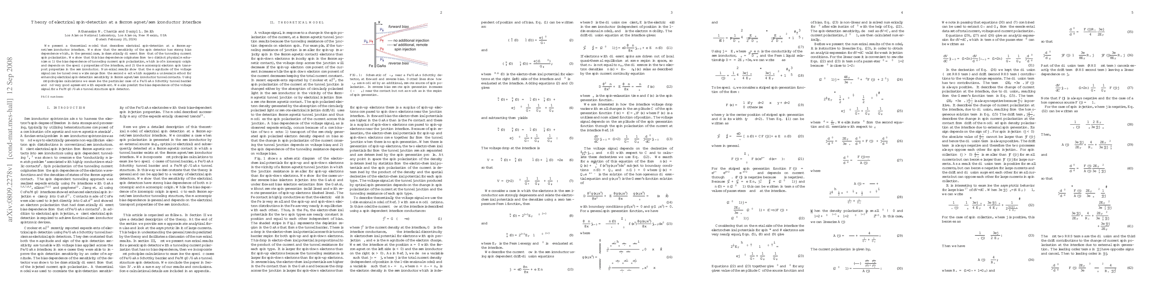
We present a theoretical model that describes electrical spin-detection at a ferromagnet/semiconductor interface. We show that the sensitivity of the spin detector has strong bias dependence which, in the general case, is dramatically different from that of the tunneling current spin polarization. We show that this bias dependence originates from two distinct physical mechanisms: 1) the bias dependence of tunneling current spin polarization, which is of microscopic origin and depends on the specific properties of the interface, and 2) the macroscopic electron spin transport properties in the semiconductor. Numerical results show that the magnitude of the voltage signal can be tuned over a wide range from the second effect which suggests a universal method for enhancing electrical spin-detection sensitivity in ferromagnet/semiconductor tunnel contacts. Using first-principles calculations we examine the particular case of a Fe/GaAs Schottky tunnel barrier and find very good agreement with experiment. We also predict the bias dependence of the voltage signal for a Fe/MgO/GaAs tunnel structure spin detector.
This graph shows how this paper is connected to other research. The current paper is shown in dark gray, papers that cite it are in green, and papers it references are in blue. You can:
• Hover over any node to see the paper title
• Click a node to view that paper's details
• Drag nodes to rearrange the graph
• Use the zoom controls (bottom right) to zoom in/out
Title | Authors | Year | Actions |
---|---|---|---|
Nonmonotonic bias dependence of local spin accumulation signals in ferromagnet/semiconductor lateral spin-valve devices
|
Y. Fujita, M. Yamada, M. Tsukahara, T. Naito, S. Yamada, K. Sawano, K. Hamaya
|
2018
|
View Paper |
Gate-tunable large magnetoresistance in an all-semiconductor spin valve device
|
M. Oltscher, F. Eberle, T. Kuczmik, A. Bayer, D. Schuh, D. Bougeard, M. Ciorga, D. Weiss
|
2017
|
View Paper |
Gate-tunable large magnetoresistance in an all-semiconductor spin-transistor-like device
|
M. Oltscher, F. Eberle, T. Kuczmik, A. Bayer, D. Schuh, D. Bougeard, M. Ciorga, D. Weiss
|
2017
|
View Paper |
Light helicity detection in MOS-based spin-photodiodes: An analytical model
|
M. Cantoni, C. Rinaldi
|
2016
|
View Paper |
In-plane tunneling anisotropic magnetoresistance in (Ga,Mn)As/GaAs Esaki diodes in the regime of the excess current
|
J. Shiogai, M. Ciorga, M. Utz, D. Schuh, M. Kohda, D. Bougeard, T. Nojima, D. Weiss, J. Nitta
|
2015
|
View Paper |
Spin and charge transport in double-junction Fe/MgO/GaAs/MgO/Fe heterostructures
|
S. Wolski, T. Szczepański, V. Dugaev, J. Barnaś, B. Landgraf, T. Slobodskyy, W. Hansen
|
2015
|
View Paper |
Electrical spin injection and detection in silicon nanowires through oxide tunnel barriers.
|
Shixiong Zhang, S. Dayeh, Yan Li, S. Crooker, Darryl L. Smith, S. Picraux
|
2013
|
View Paper |
Effect of spin drift on spin accumulation voltages in highly doped silicon
|
M. Kameno, E. Shikoh, T. Shinjo, T. Sasaki, T. Oikawa, Yoshishige Suzuki, Toshio Suzuki, M. S. O. Univ., T. Co., Ait.
|
2011
|
View Paper |
Nonmonotonic Bias-Dependent Spin Accumulation up to Room Temperature in Ferromagnet-Semiconductor Hybrid Systems
|
Y. Fujita, M. Yamada, M. Tsukahara, T. Naito, S. Yamada, S. Oki, K. Sawano, K. Hamaya
|
2018
|
View Paper |
Spin Transport in Ferromagnet/ III–V Semiconductor Heterostructures
|
2011
|
View Paper |
Published: 2007-05-23
Published: 2009-11-11
Published: 2009-07-21
Comments (0)