Publication
Metrics
AI Quick Summary
This study investigates the thickness-dependent interfacial Coulomb scattering in atomically thin MoS2 field-effect transistors, revealing a 10-fold degradation in carrier mobility for monolayer channels. The research combines experimental and theoretical approaches to show that interfacial Coulomb impurities dominate scattering in thinned channels, emphasizing the importance of surface quality for future atomic electronics.
Paper Preview
Abstract
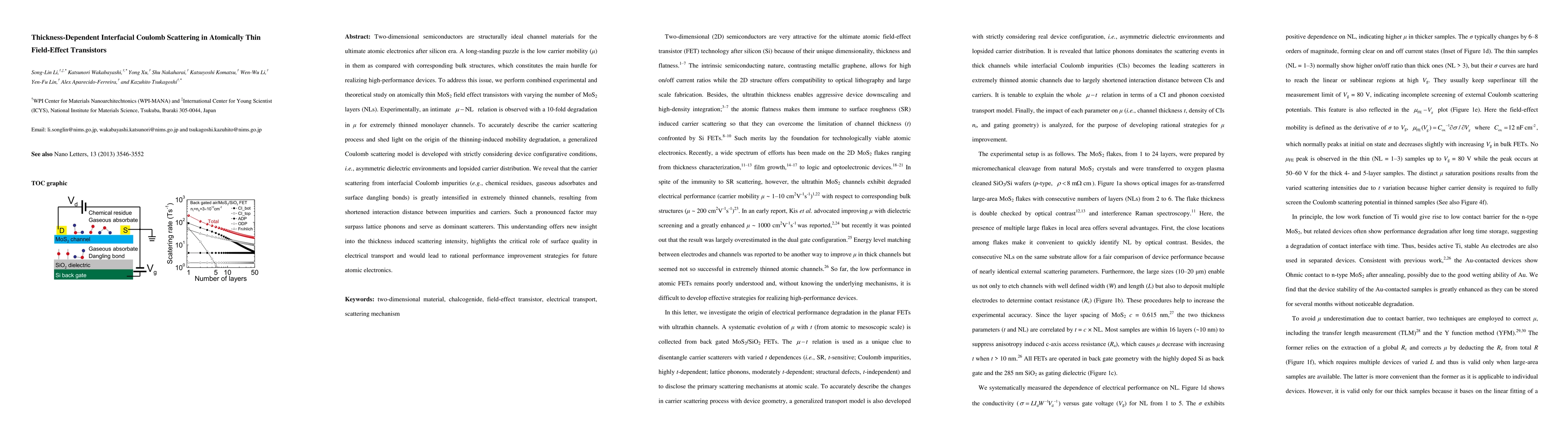
Two-dimensional semiconductors are structurally ideal channel materials for the ultimate atomic electronics after silicon era. A long-standing puzzle is the low carrier mobility ({\mu}) in them as compared with corresponding bulk structures, which constitutes the main hurdle for realizing high-performance devices. To address this issue, we perform combined experimental and theoretical study on atomically thin MoS2 field effect transistors with varying the number of MoS2 layers (NLs). Experimentally, an intimate relation is observed with a 10-fold degradation in {\mu} for extremely thinned monolayer channels. To accurately describe the carrier scattering process and shed light on the origin of the thinning-induced mobility degradation, a generalized Coulomb scattering model is developed with strictly considering device configurative conditions, i.e., asymmetric dielectric environments and lopsided carrier distribution. We reveal that the carrier scattering from interfacial Coulomb impurities (e.g., chemical residues, gaseous adsorbates and surface dangling bonds) is greatly intensified in extremely thinned channels, resulting from shortened interaction distance between impurities and carriers. Such a pronounced factor may surpass lattice phonons and serve as dominant scatterers. This understanding offers new insight into the thickness induced scattering intensity, highlights the critical role of surface quality in electrical transport and would lead to rational performance improvement strategies for future atomic electronics.
AI Key Findings
Get AI-generated insights about this paper's methodology, results, significance, and more — seven facets brought into focus.
Impact
Paper Details
PDF Preview
Key Terms
Citation Network
Current paper (gray), citations (green), references (blue)
Display is limited for performance on very large graphs.
Discussion 0