Thickness Scaling Effect on Interfacial Barrier and Electrical Contact to Two-Dimensional MoS2 Layers
Publication
Metrics
AI Quick Summary
Researchers found that the electrical contact between a metal electrode and MoS2 layers changes as the thickness of the MoS2 layer is reduced, offering a way to tailor interfacial properties for innovative functionalities.
Paper Preview
Abstract
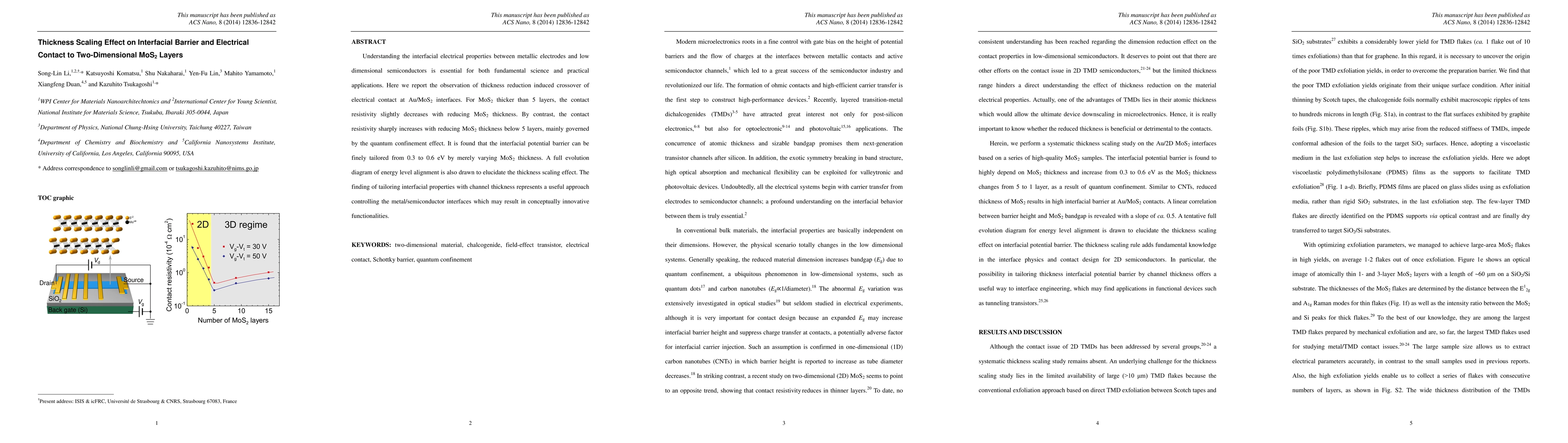
Understanding the interfacial electrical properties between metallic electrodes and low dimensional semiconductors is essential for both fundamental science and practical applications. Here we report the observation of thickness reduction induced crossover of electrical contact at Au/MoS2 interfaces. For MoS2 thicker than 5 layers, the contact resistivity slightly decreases with reducing MoS2 thickness. By contrast, the contact resistivity sharply increases with reducing MoS2 thickness below 5 layers, mainly governed by the quantum confinement effect. It is found that the interfacial potential barrier can be finely tailored from 0.3 to 0.6 eV by merely varying MoS2 thickness. A full evolution diagram of energy level alignment is also drawn to elucidate the thickness scaling effect. The finding of tailoring interfacial properties with channel thickness represents a useful approach controlling the metal/semiconductor interfaces which may result in conceptually innovative functionalities.
AI Key Findings
Get AI-generated insights about this paper's methodology, results, significance, and more — seven facets brought into focus.
Impact
Paper Details
PDF Preview
Key Terms
Citation Network
Current paper (gray), citations (green), references (blue)
Display is limited for performance on very large graphs.
Discussion 0