Thinned GaInP/GaInAs/Ge solar cells grown with reduced cracking on Ge|Si virtual substrates
Publication
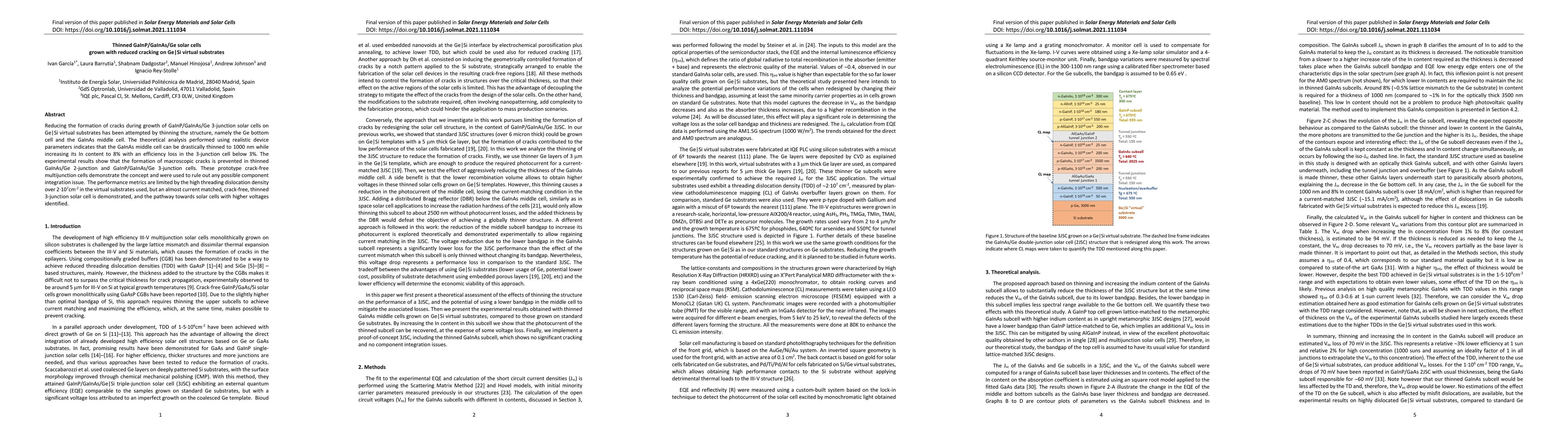
Metrics
AI Quick Summary
This paper investigates thinning the GaInAs middle cell and the Ge bottom cell in GaInP/GaInAs/Ge 3-junction solar cells to reduce cracking on Ge|Si virtual substrates, achieving crack-free prototypes with minimal efficiency loss. The high threading dislocation density in the substrates limits performance but paves the way for higher voltage solar cells.
Paper Preview
Abstract
Reducing the formation of cracks during growth of GaInP/GaInAs/Ge 3-junction solar cells on Ge|Si virtual substrates has been attempted by thinning the structure, namely the Ge bottom cell and the GaInAs middle cell. The theoretical analysis performed using realistic device parameters indicates that the GaInAs middle cell can be drastically thinned to 1000 nm while increasing its In content to 8% with an efficiency loss in the 3-junction cell below 3%. The experimental results show that the formation of macroscopic cracks is prevented in thinned GaInAs/Ge 2-junction and GaInP/GaInAs/Ge 3-junction cells. These prototype crack-free multijunction cells demonstrate the concept and were used to rule out any possible component integration issue. The performance metrics are limited by the high threading dislocation density over 2e7cm-2 in the virtual substrates used, but an almost current matched, crack-free, thinned 3-junction solar cell is demonstrated, and the pathway towards solar cells with higher voltages identified.
AI Key Findings
Get AI-generated insights about this paper's methodology, results, significance, and more — seven facets brought into focus.
Impact
Paper Details
Authors
PDF Preview
Key Terms
Citation Network
Current paper (gray), citations (green), references (blue)
Display is limited for performance on very large graphs.
Discussion 0