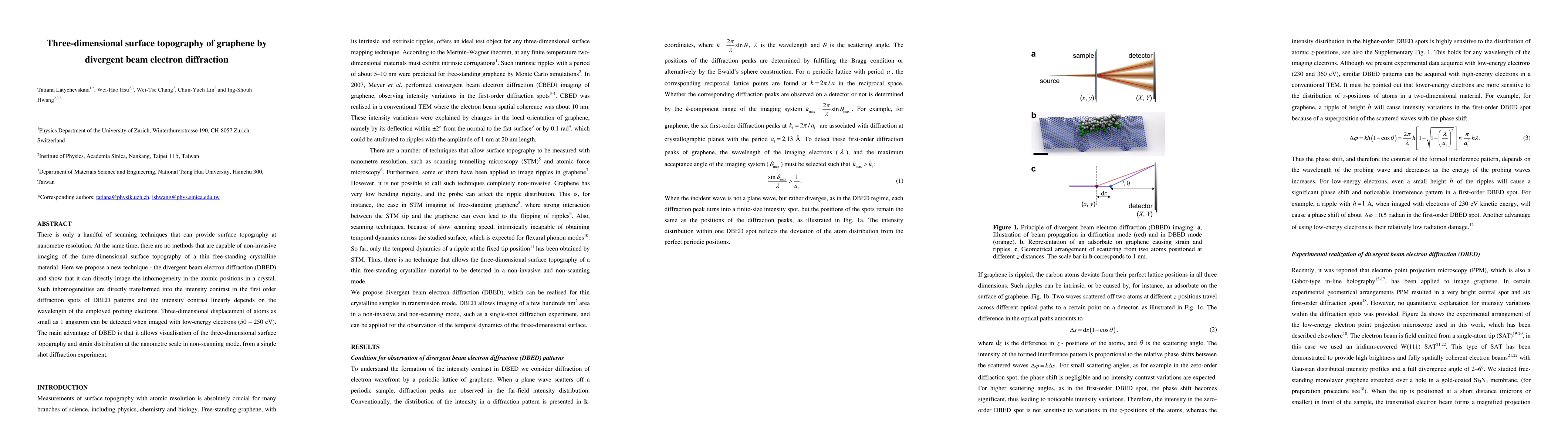
Publication
Metrics
AI Quick Summary
This paper introduces a novel technique, divergent beam electron diffraction (DBED), for non-invasive imaging of the three-dimensional surface topography of thin, free-standing crystalline materials at nanometre resolution. DBED enables visualization of atomic inhomogeneities and three-dimensional displacements as small as 1 angstrom through intensity contrast in diffraction patterns.
Paper Preview
Abstract
There is only a handful of scanning techniques that can provide surface topography at nanometre resolution. At the same time, there are no methods that are capable of non-invasive imaging of the three-dimensional surface topography of a thin free-standing crystalline material. Here we propose a new technique - the divergent beam electron diffraction (DBED) and show that it can directly image the inhomogeneity in the atomic positions in a crystal. Such inhomogeneities are directly transformed into the intensity contrast in the first order diffraction spots of DBED patterns and the intensity contrast linearly depends on the wavelength of the employed probing electrons. Three-dimensional displacement of atoms as small as 1 angstrom can be detected when imaged with low-energy electrons (50 - 250 eV). The main advantage of DBED is that it allows visualisation of the three-dimensional surface topography and strain distribution at the nanometre scale in non-scanning mode, from a single shot diffraction experiment.
AI Key Findings
Get AI-generated insights about this paper's methodology, results, significance, and more — seven facets brought into focus.
Impact
Paper Details
PDF Preview
Key Terms
Citation Network
Current paper (gray), citations (green), references (blue)
Display is limited for performance on very large graphs.
Discussion 0