This paper employs time-resolved scanning tunneling microscopy to observe negative differential resistance at the atomic scale on a silicon surface, revealing it as a many-body phenomenon linked to electron capture by a single dangling bond. The study provides detailed temporal and spatial insights into the electron dynamics involved.
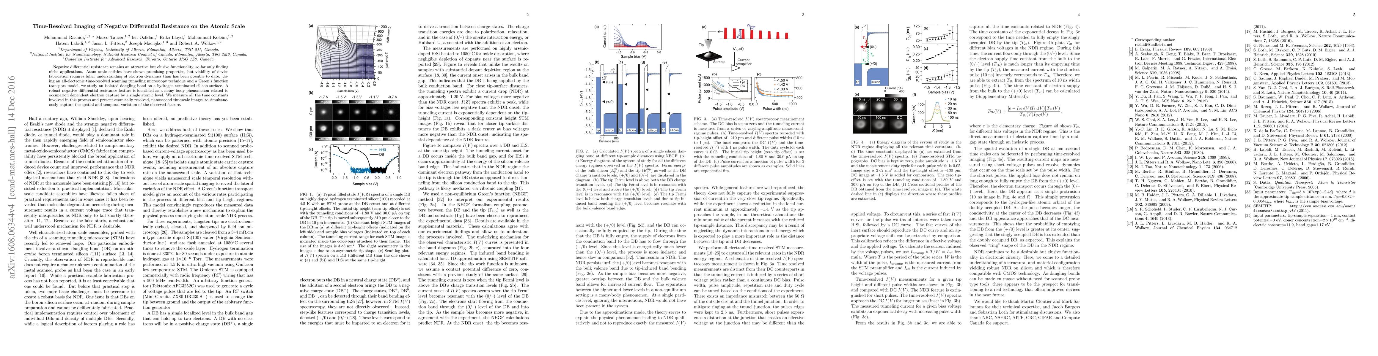
Negative differential resistance remains an attractive but elusive functionality, so far only finding niche applications. Atom scale entities have shown promising properties, but viability of device fabrication requires fuller understanding of electron dynamics than has been possible to date. Using an all-electronic time-resolved scanning tunneling microscopy technique and a Green's function transport model, we study an isolated dangling bond on a hydrogen terminated silicon surface. A robust negative differential resistance feature is identified as a many body phenomenon related to occupation dependent electron capture by a single atomic level. We measure all the time constants involved in this process and present atomically resolved, nanosecond timescale images to simultaneously capture the spatial and temporal variation of the observed feature.
This graph shows how this paper is connected to other research. The current paper is shown in dark gray, papers that cite it are in green, and papers it references are in blue. You can:
• Hover over any node to see the paper title
• Click a node to view that paper's details
• Drag nodes to rearrange the graph
• Use the zoom controls (bottom right) to zoom in/out
Title | Authors | Year | Actions |
---|---|---|---|
Electronic structures of atomic silicon dimer wires as a function of length.
|
Furkan Altincicek, L. Livadaru, Christopher C. Leon, Taras Chutora, Max Yuan, R. Achal, Jeremiah Croshaw, J. Pitters, R. Wolkow
|
2024
|
View Paper |
Spectroscopic signature of obstructed surface states in SrIn2P2
|
Xiang-Rui Liu, H.-B. Deng, Yuntian Liu, Zhou-Yang Yin, Congrun Chen, Yu-Peng Zhu, Yichen Yang, Zhicheng Jiang, Zhengtai Liu, Mao Ye, D. Shen, Jianzhuang Yin, Kedong Wang, Qihang Liu, Yuelin Zhao, Chang Liu
|
2023
|
View Paper |
Dangling bonds on the Cl- and Br-terminated Si(100) surfaces
|
T. Pavlova, V. Shevlyuga, B. V. Andryushechkin, K. Eltsov
|
2022
|
View Paper |
Magnetic tunneling junctions based on 2D CrI3 and CrBr3: spin-filtering effects and high tunnel magnetoresistance via energy band difference
|
Li Liu, Shizhuo Ye, Jin He, Qijun Huang, Hao Wang, Sheng Chang
|
2021
|
View Paper |
Recent Progress on the Scanning Tunneling Microscopy and Spectroscopy Study of Semiconductor Heterojunctions.
|
W. Peng, Haolin Wang, Hui Lu, L. Yin, Yue Wang, B. Grandidier, Deren Yang, X. Pi
|
2021
|
View Paper |
Ionic charge distributions in silicon atomic surface wires.
|
Jeremiah Croshaw, Taleana R Huff, M. Rashidi, J. Wood, Erika Lloyd, J. Pitters, R. Wolkow
|
2021
|
View Paper |
Negative Pulse and Compliance Current Dependent Negative Differential Resistance in ZnO/Nb:SrTiO3 Heterojunctions
|
Qinxuan Li, C. Jia, Yong Ren, Ying Zhang, Weifeng Zhang
|
2021
|
View Paper |
Ring charging of a single silicon dangling bond imaged by noncontact atomic force microscopy
|
N. Turek, S. Godey, D. Deresmes, T. Mélin
|
2020
|
View Paper |
Gigahertz Frame Rate Imaging of Charge-Injection Dynamics in a Molecular Light Source
|
Anna Rosławska, P. Merino, Christopher C. Leon, Abhishek Grewal, M. Etzkorn, K. Kuhnke, K. Kern
|
2020
|
View Paper |
Imaging of nearly flat band induced atomic-scale negative differential conductivity in
ABC
-stacked trilayer graphene
|
Long-Jing Yin, Li-Zhen Yang, Li Zhang, Qilong Wu, Xiaoshuai Fu, L. Tong, Guang Yang, Yuan Tian, Lijie Zhang, Zhihui Qin
|
2020
|
View Paper |
Ionic Charge Distributions in Silicon Atomic Wires
|
Jeremiah Croshaw, Taleana R Huff, M. Rashidi, J. Wood, Erika Lloyd, J. Pitters, R. Wolkow
|
2020
|
View Paper |
Significant tunneling magnetoresistance and excellent spin filtering effect in CrI3-based van der Waals magnetic tunnel junctions.
|
Zhi Yan, Ruiqiang Zhang, Xinlong Dong, S. Qi, Xiaohong Xu
|
2020
|
View Paper |
Current-Induced Thermal Tunneling Electroluminescence in a Single Highly Compensated Semiconductor Microrod
|
C. Xing, Wei Liu, Qiang Wang, Chunxiang Xu, Yinzhou Yan, Yi-jian Jiang
|
2020
|
View Paper |
Temperature- and pulse-dependent negative differential resistances in ZnO/Nb:SrTiO3 heterojunctions
|
C. Jia, Yong Ren, Yanfeng Yin, Weifeng Zhang
|
2019
|
View Paper |
Negative differential conductance in the electron-transport through copper-rich cuprous oxide thin films
|
A. Gloystein, C. Möller, N. Nilius
|
2019
|
View Paper |
Atomic‐Scale Manipulation and In Situ Characterization with Scanning Tunneling Microscopy
|
Wonhee Ko, Chuanxu Ma, G. Nguyen, M. Kolmer, An‐Ping Li
|
2019
|
View Paper |
Tuning the charge flow between Marcus regimes in an organic thin-film device
|
A. Atxabal, Thorsten Arnold, S. Parui, S. Hutsch, Elisabetta Zuccatti, R. Llopis, M. Cinchetti, F. Casanova, F. Ortmann, L. Hueso
|
2019
|
View Paper |
Trap-Free Heterostructure of PbS Nanoplatelets on InP(001) by Chemical Epitaxy.
|
L. Biadala, W. Peng, Y. Lambert, Jin Ho Kim, D. Canneson, Anthony Houppe, M. Berthe, D. Troadec, D. Deresmes, G. Patriarche, T. Xu, X. Pi, X. Wallart, C. Delerue, M. Bayer, Jimmy Xu, B. Grandidier
|
2019
|
View Paper |
Remarkable negative differential resistance and perfect spin-filtering effects of the indium triphosphide (InP3) monolayer tuned by electric and optical ways.
|
Shenghui Zhang, Yiqun Xie, Yibin Hu, X. Niu, Yin Wang
|
2018
|
View Paper |
Design of Atomically Precise Nanoscale Negative Differential Resistance Devices
|
Zhongcan Xiao, Chuanxu Ma, Jingsong Huang, L. Liang, Wenchang Lu, K. Hong, B. Sumpter, An‐Ping Li, J. Bernholc
|
2018
|
View Paper |
Modulation of Negative Differential Resistance in Graphene Field-Effect Transistors by Tuning the Contact Resistances
|
P. Tran
|
2018
|
View Paper |
Single Charge and Exciton Dynamics Probed by Molecular-Scale-Induced Electroluminescence.
|
Anna Rosławska, P. Merino, C. Große, Christopher C. Leon, O. Gunnarsson, M. Etzkorn, K. Kuhnke, K. Kern
|
2018
|
View Paper |
Autonomous Scanning Probe Microscopy in Situ Tip Conditioning through Machine Learning.
|
M. Rashidi, R. Wolkow
|
2018
|
View Paper |
Negative differential conductance in doped-silicon nanoscale devices with superconducting electrodes
|
A. Shapovalov, V. Shaternik, O. Suvorov, E. Zhitlukhina, M. Belogolovskii
|
2018
|
View Paper |
Magnetic-field-controlled negative differential conductance in scanning tunneling spectroscopy of graphene npn junction resonators
|
Si-Yu Li, Haiwen Liu, Jiabin Qiao, Hua Jiang, Lin He
|
2017
|
View Paper |
Resolving and Tuning Carrier Capture Rates at a Single Silicon Atom Gap State.
|
M. Rashidi, Erika Lloyd, Taleana R Huff, R. Achal, M. Taucer, Jeremiah Croshaw, R. Wolkow
|
2017
|
View Paper |
Supramolecular self-assembly on the B-Si(111)-(√3x√3) R30° surface: From single molecules to multicomponent networks
|
Y. Makoudi, J. Jeannoutot, F. Palmino, F. Chérioux, G. Copie, C. Krzeminski, F. Cleri, B. Grandidier
|
2017
|
View Paper |
Tip-induced passivation of dangling bonds on hydrogenated Si(100)-2 × 1
|
N. Pavliček, Z. Majzik, G. Meyer, L. Gross
|
2017
|
View Paper |
Toward Atom Scale Ultra Low Power Classical Circuitry and Quantum Circuitry
|
R. Wolkow
|
2017
|
View Paper |
All-electronic Nanosecond-resolved Scanning Tunneling Microscopy: Facilitating the Investigation of Single Dopant Charge Dynamics.
|
M. Rashidi, Wyatt Vine, J. Burgess, M. Taucer, R. Achal, J. Pitters, S. Loth, R. Wolkow
|
2017
|
View Paper |
Optimizing surface defects for atomic-scale electronics: Si dangling bonds
|
P. Scherpelz, G. Galli
|
2017
|
View Paper |
Ultrafast terahertz control of extreme tunnel currents through single atoms on a silicon surface
|
V. Jelic, K. Iwaszczuk, P. Nguyen, C. Rathje, G. Hornig, H. Sharum, J. R. Hoffman, M. R. Freeman, F. Hegmann
|
2017
|
View Paper |
基于强场太赫兹脉冲的扫描隧道显微镜
|
谷建强 Gu Jianqiang, 安有文 An Youwen
|
2023
|
View Paper |
Materials at Atomic Scale
|
M. Dragoman, D. Dragoman
|
2020
|
View Paper |
Dynamics of nanoscale systems probed by time-resolved STM-induced luminescence
|
Anna Rosławska
|
2019
|
View Paper |
In-device spectroscopy at metal/organic semiconductor interfaces
|
A. Atxabal
|
2018
|
View Paper |
Published: 2019-01-03
Yi Cai, Jingzhen Li, Xuanke Zeng, Xiaowei Lu, Qifan Zhu, Yongle Zhu
Published: 2023-10-19
Comments (0)