Publication
Metrics
AI Quick Summary
This study employs scanning tunneling microscopy and density functional theory to visualize the 3x3 charge density wave in 2H-NbSe2, revealing its spatial distribution across different layers. The charge order strength varies with tunneling current, showing a phase shift correlated with Se p and Nb d orbital distributions.
Paper Preview
Abstract
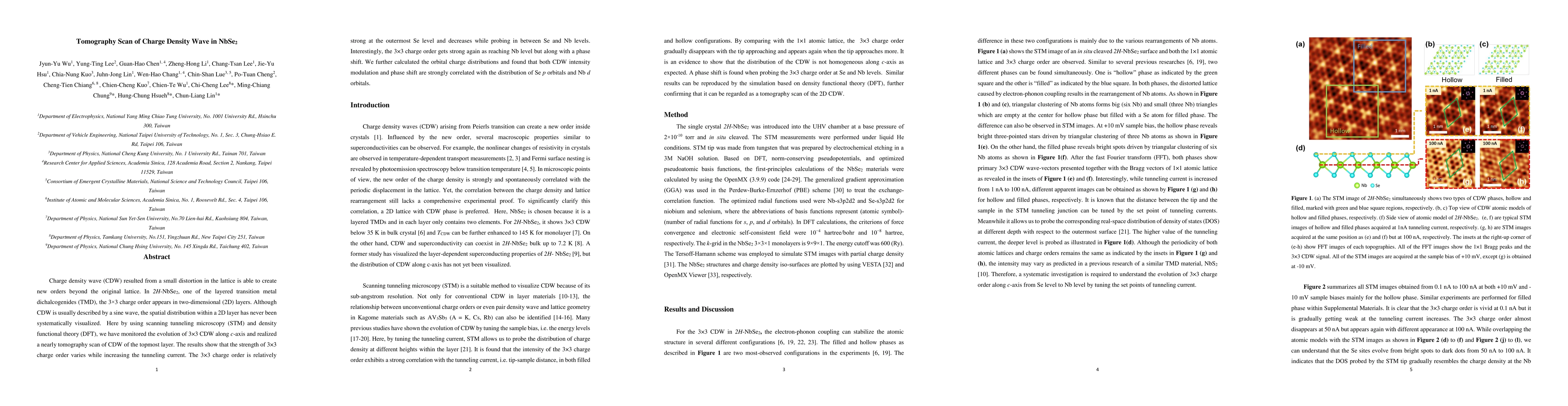
Charge density wave (CDW) resulted from a small distortion in the lattice is able to create new orders beyond the original lattice. In 2H-NbSe2, one of the layered transition metal dichalcogenides (TMD), the 3x3 charge order appears in two-dimensional (2D) layers. Although CDW is usually described by a sine wave, the spatial distribution within a 2D layer has never been systematically visualized. Here by using scanning tunneling microscopy (STM) and density functional theory (DFT), we have monitored the evolution of 3x3 CDW along c-axis and realized a nearly tomography scan of CDW of the topmost layer. The results show that the strength of 3x3 charge order varies while increasing the tunneling current. The 3x3 charge order is relatively strong at the outermost Se level and decreases while probing in between Se and Nb levels. Interestingly, the 3x3 charge order gets strong again as reaching Nb level but along with a phase shift. We further calculated the orbital charge distributions and found that both CDW intensity modulation and phase shift are strongly correlated with the distribution of Se p orbitals and Nb d orbitals.
AI Key Findings
Get AI-generated insights about this paper's methodology, results, significance, and more — seven facets brought into focus.
Paper Details
Authors
PDF Preview
Key Terms
Related Papers
No references found for this paper.
Discussion 0