Publication
Metrics
AI Quick Summary
This paper presents a scalable top-down fabrication method for bulk-insulating topological insulator nanowires (TINWs) from high-quality thin films, enabling tuning of the chemical potential to the charge neutrality point. The study demonstrates characteristic topological subband physics and the superconducting proximity effect, laying the foundation for future quantum devices based on Majorana bound states.
Paper Preview
Abstract
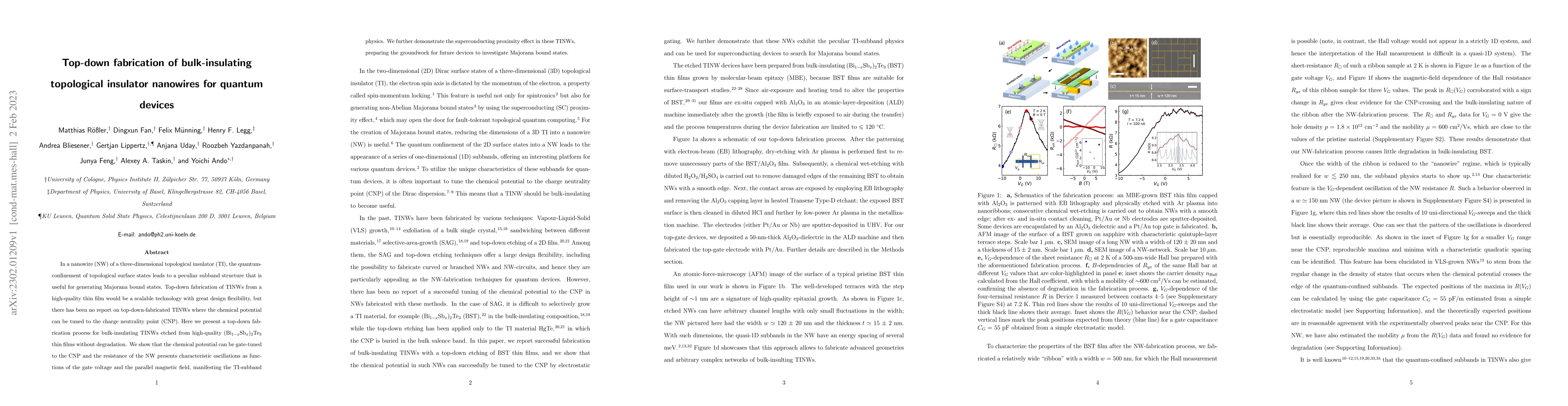
In a nanowire (NW) of a three-dimensional topological insulator (TI), the quantum-confinement of topological surface states leads to a peculiar subband structure that is useful for generating Majorana bound states. Top-down fabrication of TINWs from a high-quality thin film would be a scalable technology with great design flexibility, but there has been no report on top-down-fabricated TINWs where the chemical potential can be tuned to the charge neutrality point (CNP). Here we present a top-down fabrication process for bulk-insulating TINWs etched from high-quality (Bi$_{1-x}$Sb$_{x}$)$_2$Te$_3$ thin films without degradation. We show that the chemical potential can be gate-tuned to the CNP and the resistance of the NW presents characteristic oscillations as functions of the gate voltage and the parallel magnetic field, manifesting the TI-subband physics. We further demonstrate the superconducting proximity effect in these TINWs, preparing the groundwork for future devices to investigate Majorana bound states.
AI Key Findings
Get AI-generated insights about this paper's methodology, results, significance, and more — seven facets brought into focus.
Impact
Paper Details
Authors
PDF Preview
Key Terms
Citation Network
Current paper (gray), citations (green), references (blue)
Display is limited for performance on very large graphs.
Discussion 0