Topological Dislocation Response in Elementary Semiconductors

PDF

Publication

Published: Feb 24, 2026
Categories: cond-mat.mes-hall

Metrics

Source: ArXiv

Quick Actions

View PDF

Quick Answers

What methodology did the authors use?

The authors combine symmetry indicator analysis (weak SSH invariants) with tight‑binding simulations of realistic crystal models to compute band structures in the presence of dislocations. More in Methodology →

What are the key results?

Edge dislocations in inversion‑symmetric semiconductors host topologically protected mid‑gap polarization bands, while screw dislocations are trivial. — Weak SSH invariants correctly predict the presence or absence of dislocation‑bound states in silicon, diamond, germanium, and black phosphorene. More in Key Results →

Why is this work significant?

The work shows that ubiquitous semiconductors can support robust dislocation‑bound modes, providing a new probe of topological properties and potential for defect‑based electronic functionalities. More in Significance →

What are the main limitations?

The analysis is limited to inversion‑symmetric materials and I‑symmetric dislocations. — Tight‑binding models neglect many‑body interactions and disorder effects that could modify the dislocation spectrum. More in Limitations →

Paper Preview

Abstract

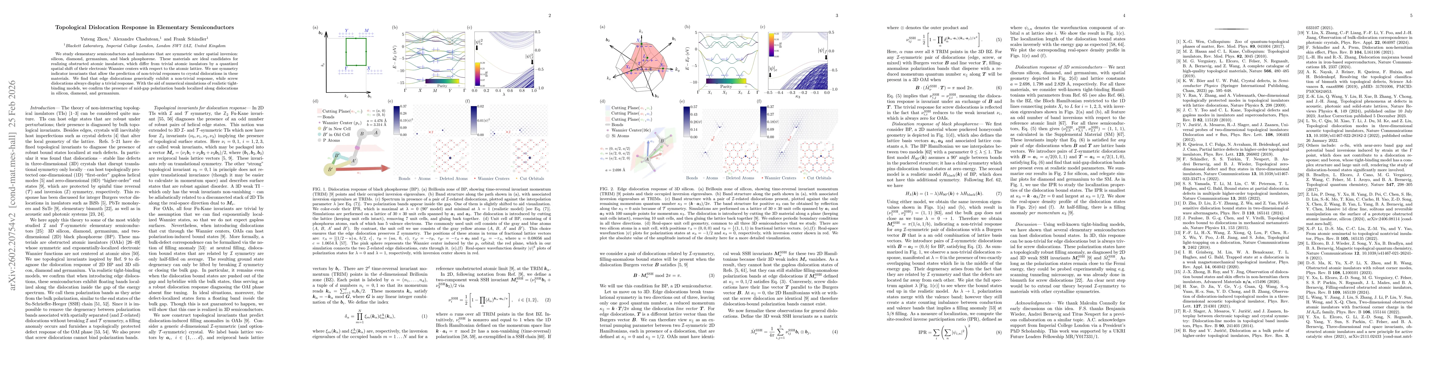
We study elementary semiconductors and insulators that are symmetric under spatial inversion: silicon, diamond, germanium, and black phosphorene. These materials are ideal candidates for realizing obstructed atomic insulators, which differ from trivial atomic insulators by a quantized spatial shift of their electronic Wannier centers with respect to the atomic lattice. We use symmetry indicator invariants that allow the prediction of non-trivial responses to crystal dislocations in these materials. We find that edge dislocations generically exhibit a non-trivial response, while screw dislocations always display a trivial response. With the aid of numerical simulations of realistic tight-binding models, we confirm the presence of mid-gap polarization bands localized along dislocations in silicon, diamond, and germanium.

AI Key Findings

Generated Feb 26, 2026

Methodology — What approach did the authors take?

The authors combine symmetry indicator analysis (weak SSH invariants) with tight‑binding simulations of realistic crystal models to compute band structures in the presence of dislocations.

Key Results — What are the main findings?

  • Edge dislocations in inversion‑symmetric semiconductors host topologically protected mid‑gap polarization bands, while screw dislocations are trivial.
  • Weak SSH invariants correctly predict the presence or absence of dislocation‑bound states in silicon, diamond, germanium, and black phosphorene.
  • Numerical tight‑binding calculations confirm the existence of these mid‑gap states and reveal a filling anomaly at half‑filling.

Significance — Why does this research matter?

The work shows that ubiquitous semiconductors can support robust dislocation‑bound modes, providing a new probe of topological properties and potential for defect‑based electronic functionalities.

Technical Contribution — What is the technical contribution?

Introduction of weak SSH invariants as symmetry indicators for predicting dislocation responses in obstructed atomic insulators, and systematic tight‑binding validation across several elemental semiconductors.

Novelty — What is new about this work?

First systematic use of symmetry indicators to predict and confirm dislocation‑bound states in common elemental semiconductors, revealing non‑trivial edge‑dislocation physics that had not been previously identified.

Limitations — What are the limitations of this study?

  • The analysis is limited to inversion‑symmetric materials and I‑symmetric dislocations.
  • Tight‑binding models neglect many‑body interactions and disorder effects that could modify the dislocation spectrum.

Future Work — What did the authors propose for future work?

  • Extend the symmetry‑indicator framework to crystals with other point‑group symmetries.
  • Perform experimental STM or transport studies to detect the predicted dislocation states in silicon and diamond.

Paper Details

Paper ID: 2602.20754
Categories:
cond-mat.mes-hall

How to Cite This Paper

BibTeX
@article{chaduteau2026topological,
  title         = {Topological Dislocation Response in Elementary Semiconductors},
  author        = {Chaduteau, Alexandre and Schindler, Frank and Zhou, Yuteng},
  year          = {2026},
  eprint        = {2602.20754},
  archivePrefix = {arXiv},
  primaryClass  = {cond-mat.mes-hall},
}
APA 7
Chaduteau, A., Schindler, F., & Zhou, Y. (2026). Topological Dislocation Response in Elementary Semiconductors. arXiv. https://arxiv.org/abs/2602.20754
MLA 9
Chaduteau, Alexandre, et al. "Topological Dislocation Response in Elementary Semiconductors." arXiv, 2026, arxiv.org/abs/2602.20754.

Comments (0)

This website uses cookies to ensure you get the best experience. Learn more