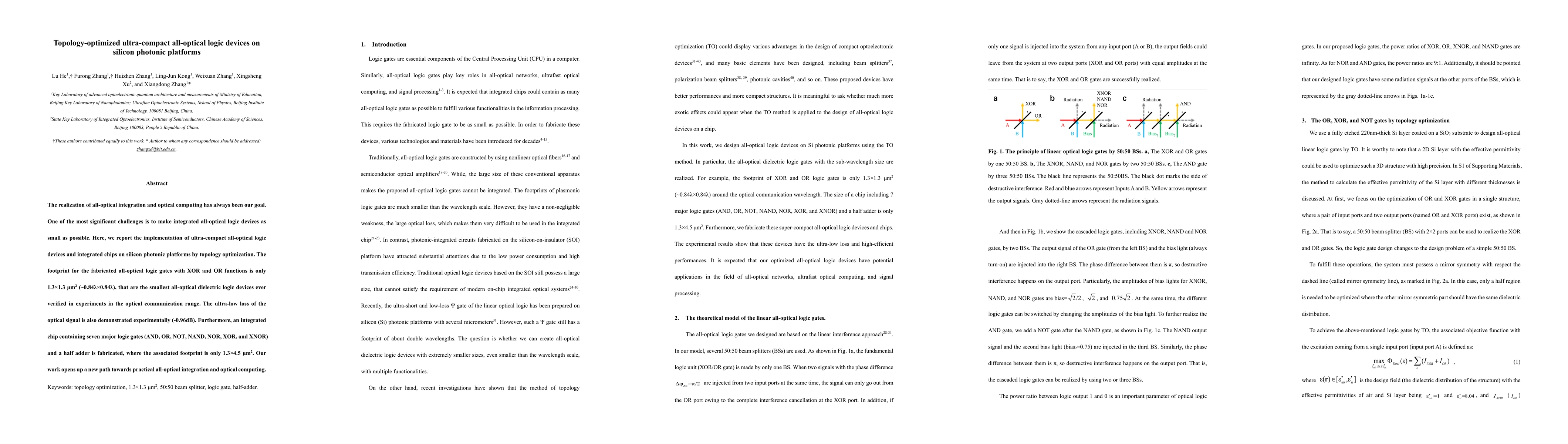
Topology-optimized ultra-compact all-optical logic devices on silicon photonic platforms
Publication
Metrics
AI Quick Summary
This paper presents ultra-compact all-optical logic devices on silicon photonic platforms achieved through topology optimization, achieving the smallest footprint for XOR and OR gates ever verified experimentally. The devices demonstrate ultra-low optical signal loss and pave the way for practical all-optical integration and computing.
Paper Preview
Abstract
The realization of all-optical integration and optical computing has always been our goal. One of the most significant challenges is to make integrated all-optical logic devices as small as possible. Here, we report the implementation of ultra-compact all-optical logic devices and integrated chips on silicon photonic platforms by topology optimization. The footprint for the fabricated all-optical logic gates with XOR and OR functions is only 1.3*1.3 {\mu}m2 (~0.84{\lambda}*0.84{\lambda}), that are the smallest all-optical dielectric logic devices ever verified in experiments in the optical communication range. The ultra-low loss of the optical signal is also demonstrated experimentally (-0.96dB). Furthermore, an integrated chip containing seven major logic gates (AND, OR, NOT, NAND, NOR, XOR, and XNOR) and a half adder is fabricated, where the associated footprint is only 1.3*4.5 {\mu}m2. Our work opens up a new path towards practical all-optical integration and optical computing.
AI Key Findings
Get AI-generated insights about this paper's methodology, results, significance, and more — seven facets brought into focus.
Impact
Paper Details
Authors
PDF Preview
Key Terms
Citation Network
Current paper (gray), citations (green), references (blue)
Display is limited for performance on very large graphs.
Discussion 0