Summary

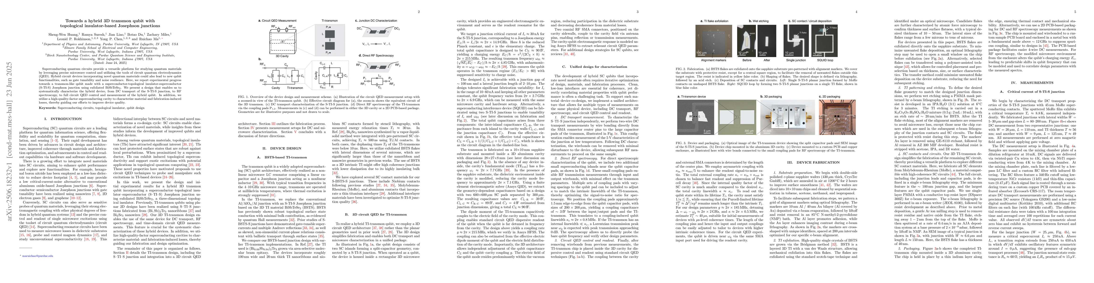
Superconducting quantum circuits provide a versatile platform for studying quantum materials by leveraging precise microwave control and utilizing the tools of circuit quantum electrodynamics (QED). Hybrid circuit devices incorporating novel quantum materials could also lead to new qubit functionalities, such as gate tunability and noise resilience. Here, we report experimental progress towards a transmon-like qubit made with a superconductor-topological insulator-superconductor (S-TI-S) Josephson junction using exfoliated BiSbTeSe2. We present a design that enables us to systematically characterize the hybrid device, from DC transport of the S-TI-S junction, to RF spectroscopy, to full circuit QED control and measurement of the hybrid qubit. In addition, we utilize a high-quality-factor superconducting cavity to characterize material and fabrication-induced losses, thereby guiding our efforts to improve device quality.

AI Key Findings

Generated Sep 03, 2025

Methodology

The research presents a fabrication process for a hybrid 3D transmon qubit using a superconductor-topological insulator-superconductor (S-TI-S) Josephson junction with exfoliated BiSbTeSe2. The methodology includes exfoliation, wet etching, deposition of superconducting contacts and circuits, and packaging.

Key Results

  • Successful fabrication and characterization of S-TI-S Josephson junctions with critical currents significantly smaller than the BCS superconducting gap of MoRe, indicating low effective junction transparency.
  • Design and implementation of an RF measurement setup using an open-source Quantum Instrument Control Kit (QICK) built on Xilinx RFSoC hardware for future circuit-QED control and readout of the hybrid TI-transmon qubit.
  • Characterization of microwave losses in the hybrid devices using high-Q superconducting cavities, revealing that the etching procedure does not introduce significant additional loss.

Significance

This research provides a unified framework for DC transport, RF spectroscopy, and circuit-QED measurements on a single device, facilitating the efficient co-design of materials, fabrication processes, and qubit architectures for hybrid quantum devices.

Technical Contribution

The paper presents a novel hybrid 3D transmon qubit design incorporating topological insulator materials and a comprehensive fabrication process for such devices.

Novelty

This work introduces a hybrid quantum system leveraging topological insulator materials for potential noise-resilience and new functionalities in quantum information processing, along with a detailed fabrication methodology for such hybrid devices.

Limitations

  • The study does not yet demonstrate qubit operation or significant coherence times.
  • The research focuses on characterizing individual components and does not explore full qubit control or readout.

Future Work

  • Integration of electrostatic gates to enable in situ voltage control of the critical current of the S-TI-S junction for fast qubit frequency tuning.
  • Incorporation of on-chip LC low-pass filters on the gate control line to mitigate Purcell decay and enhance coherence times.

Paper Details

PDF Preview

Download PDF

Citation Network

Current paper (gray), citations (green), references (blue)

Display is limited for performance on very large graphs.

Current Paper
Citations
References
Click to view

No citations found for this paper.

Comments (0)

This website uses cookies to ensure you get the best experience. Learn more