Transfer of Large-Scale Two-Dimensional Semiconductors: Challenges and Developments
Publication
Metrics
Paper Preview
Abstract
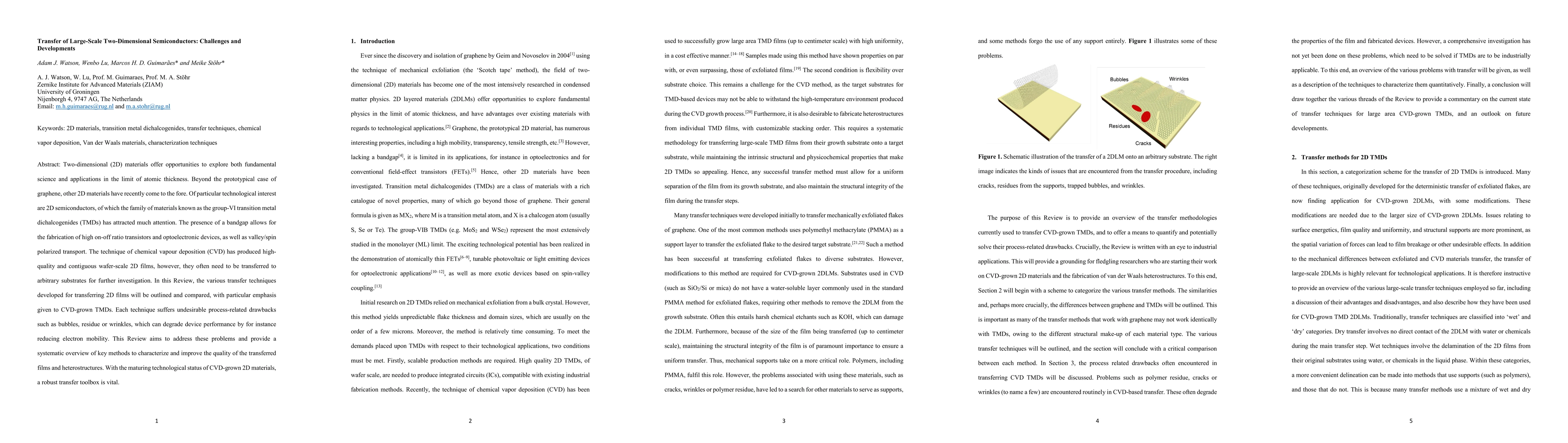
Two-dimensional (2D) materials offer opportunities to explore both fundamental science and applications in the limit of atomic thickness. Beyond the prototypical case of graphene, other 2D materials have recently come to the fore. Of particular technological interest are 2D semiconductors, of which the family of materials known as the group-VI transition metal dichalcogenides (TMDs) has attracted much attention. The presence of a bandgap allows for the fabrication of high on-off ratio transistors and optoelectronic devices, as well as valley/spin polarized transport. The technique of chemical vapour deposition (CVD) has produced high-quality and contiguous wafer-scale 2D films, however, they often need to be transferred to arbitrary substrates for further investigation. In this Review, the various transfer techniques developed for transferring 2D films will be outlined and compared, with particular emphasis given to CVD-grown TMDs. Each technique suffers undesirable process-related drawbacks such as bubbles, residue or wrinkles, which can degrade device performance by for instance reducing electron mobility. This Review aims to address these problems and provide a systematic overview of key methods to characterize and improve the quality of the transferred films and heterostructures. With the maturing technological status of CVD-grown 2D materials, a robust transfer toolbox is vital.
AI Key Findings
Get AI-generated insights about this paper's methodology, results, significance, and more — seven facets brought into focus.
Impact
Paper Details
Authors
PDF Preview
Key Terms
Citation Network
Current paper (gray), citations (green), references (blue)
Display is limited for performance on very large graphs.
Discussion 0