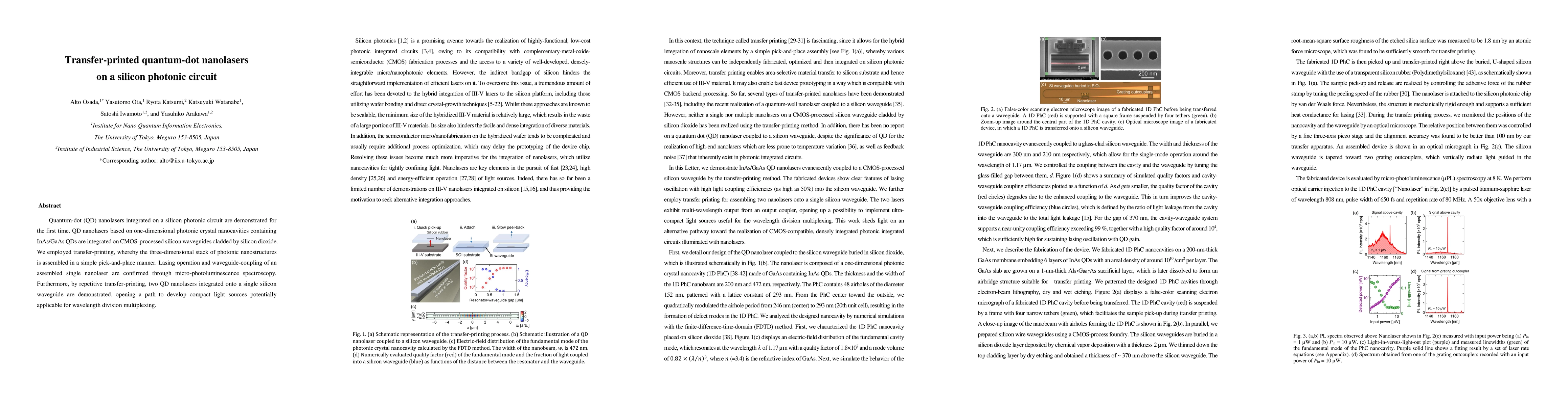
Publication
Metrics
AI Quick Summary
This paper demonstrates the first integration of quantum-dot nanolasers on a silicon photonic circuit using transfer-printing. The nanolasers, based on InAs/GaAs quantum dots within photonic crystal nanocavities, are coupled to CMOS-processed silicon waveguides, enabling lasing operation and paving the way for compact, multiplexed light sources.
Paper Preview
Abstract
Quantum-dot (QD) nanolasers integrated on a silicon photonic circuit are demonstrated for the first time. QD nanolasers based on one-dimensional photonic crystal nanocavities containing InAs/GaAs QDs are integrated on CMOS-processed silicon waveguides cladded by silicon dioxide. We employed transfer-printing, whereby the three-dimensional stack of photonic nanostructures is assembled in a simple pick-and-place manner. Lasing operation and waveguide-coupling of an assembled single nanolaser are confirmed through micro-photoluminescence spectroscopy. Furthermore, by repetitive transfer-printing, two QD nanolasers integrated onto a single silicon waveguide are demonstrated, opening a path to develop compact light sources potentially applicable for wavelength division multiplexing.
AI Key Findings
Get AI-generated insights about this paper's methodology, results, significance, and more — seven facets brought into focus.
Impact
Paper Details
PDF Preview
Key Terms
Citation Network
Current paper (gray), citations (green), references (blue)
Display is limited for performance on very large graphs.
Discussion 0