Publication
Metrics
AI Quick Summary
This paper presents a scalable dry transfer method for CVD graphene to pre-patterned substrates, achieving nearly zero Dirac voltage and low contact resistance, enabling high-sensitivity graphene FET biosensors. The resist-free process ensures a clean graphene surface and allows for conducting channel lengths up to one millimeter.
Paper Preview
Abstract
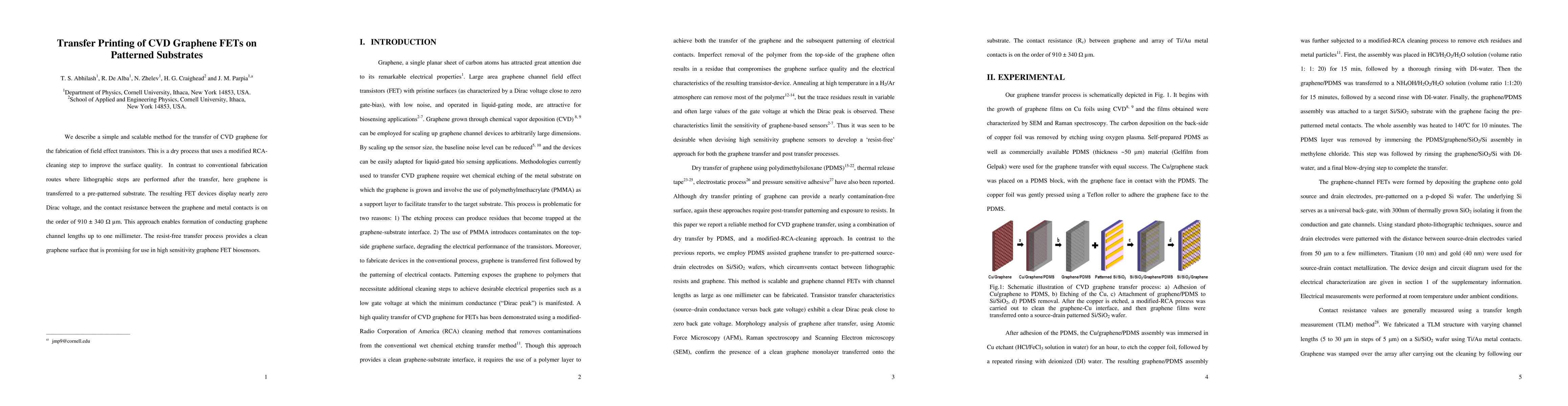
We describe a simple and scalable method for the transfer of CVD graphene for the fabrication of field effect transistors. This is a dry process that uses a modified RCA cleaning step to improve the surface quality. In contrast to conventional fabrication routes where lithographic steps are performed after the transfer, here graphene is transferred to a pre-patterned substrate. The resulting FET devices display nearly zero Dirac voltage, and the contact resistance between the graphene and metal contacts is on the order of 910 +- 340 Ohm-micrometer. This approach enables formation of conducting graphene channel lengths up to one millimeter. The resist-free transfer process provides a clean graphene surface that is promising for use in high sensitivity graphene FET biosensors.
AI Key Findings
Get AI-generated insights about this paper's methodology, results, significance, and more — seven facets brought into focus.
Impact
Paper Details
PDF Preview
Key Terms
Citation Network
Current paper (gray), citations (green), references (blue)
Display is limited for performance on very large graphs.
Discussion 0