Transport of topologically protected photonic waveguide on chip
Publication
Metrics
AI Quick Summary
This paper introduces a novel topologically protected photonic waveguide on an integrated chip, utilizing a photonic crystal design with Dirac points. The design maintains valley-locking and defect immunity, enabling enhanced integrated photonic devices such as superior energy concentrators and customizable photonic power splitters.
Paper Preview
Abstract
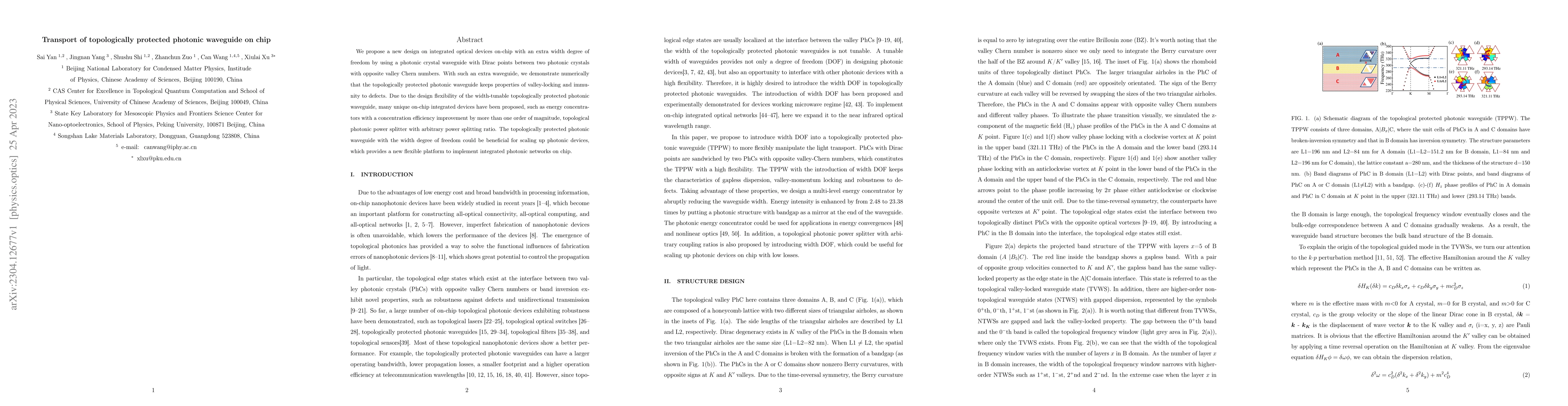
We propose a new design on integrated optical devices on-chip with an extra width degree of freedom by using a photonic crystal waveguide with Dirac points between two photonic crystals with opposite valley Chern numbers. With such an extra waveguide, we demonstrate numerically that the topologically protected photonic waveguide keeps properties of valley-locking and immunity to defects. Due to the design flexibility of the width-tunable topologically protected photonic waveguide, many unique on-chip integrated devices have been proposed, such as energy concentrators with a concentration efficiency improvement by more than one order of magnitude, topological photonic power splitter with arbitrary power splitting ratio. The topologically protected photonic waveguide with the width degree of freedom could be beneficial for scaling up photonic devices, which provides a new flexible platform to implement integrated photonic networks on chip.
AI Key Findings
Get AI-generated insights about this paper's methodology, results, significance, and more — seven facets brought into focus.
Impact
Paper Details
Authors
PDF Preview
Key Terms
Citation Network
Current paper (gray), citations (green), references (blue)
Display is limited for performance on very large graphs.
Discussion 0