Summary
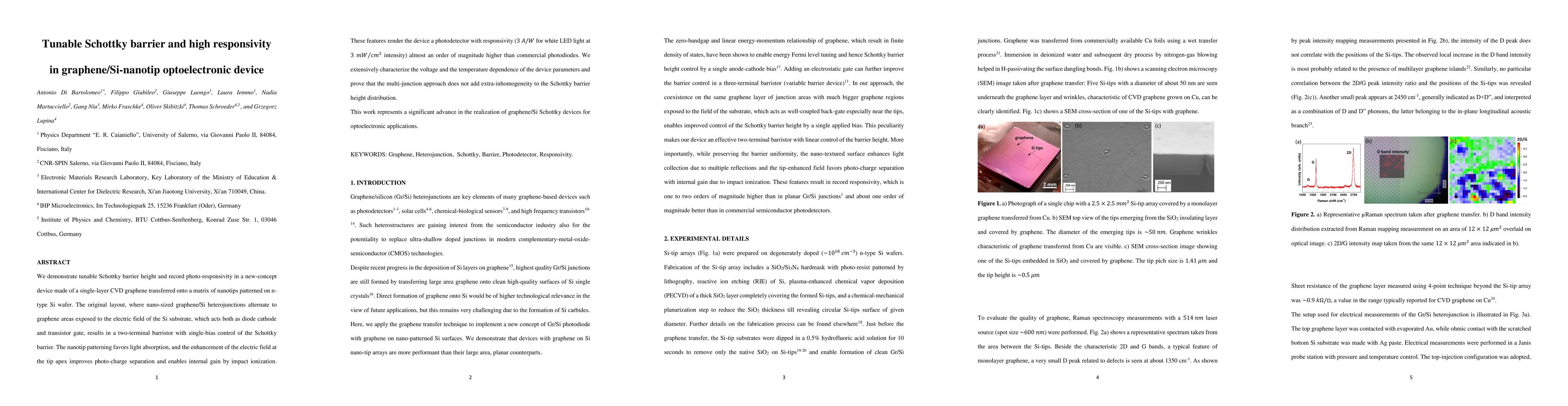
We demonstrate tunable Schottky barrier height and record photo-responsivity in a new-concept device made of a single-layer CVD graphene transferred onto a matrix of nanotips patterned on n-type Si wafer. The original layout, where nano-sized graphene/Si heterojunctions alternate to graphene areas exposed to the electric field of the Si substrate, which acts both as diode cathode and transistor gate, results in a two-terminal barristor with single-bias control of the Schottky barrier. The nanotip patterning favors light absorption, and the enhancement of the electric field at the tip apex improves photo-charge separation and enables internal gain by impact ionization. These features render the device a photodetector with responsivity (3 A/W for white LED light at 3 mW/cm2 intensity) almost an order of magnitude higher than commercial photodiodes. We extensively characterize the voltage and the temperature dependence of the device parameters and prove that the multi-junction approach does not add extra-inhomogeneity to the Schottky barrier height distribution. This work represents a significant advance in the realization of graphene/Si Schottky devices for optoelectronic applications.
AI Key Findings
Get AI-generated insights about this paper's methodology, results, and significance.
Paper Details
PDF Preview
Key Terms
Citation Network
Current paper (gray), citations (green), references (blue)
Display is limited for performance on very large graphs.
Similar Papers
Found 4 papersGraphene/SOI-based self-powered Schottky barrier photodiode array
M. Fidan, A. Yanilmaz, O. Unverdi et al.
| Title | Authors | Year | Actions |
|---|
Comments (0)