Publication
Metrics
AI Quick Summary
This study measures the thermal conductivity of InAs nanowires, showing it is significantly lower than bulk values due to phonon localization in twin-defects. The thermal conductivity is tunable via electrostatic gating and magnetic fields, revealing the influence of surface accumulation layers on nanoscale thermal transport.
Paper Preview
Abstract
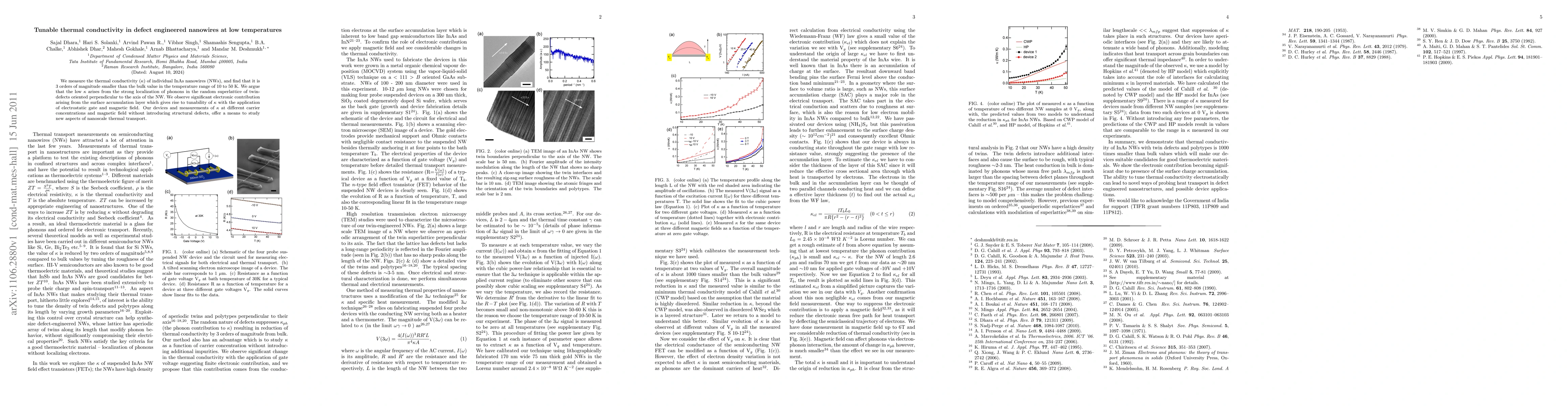
We measure the thermal conductivity ($\kappa$) of individual InAs nanowires (NWs), and find that it is 3 orders of magnitude smaller than the bulk value in the temperature range of 10 to 50 K. We argue that the low $\kappa$ arises from the strong localization of phonons in the random superlattice of twin-defects oriented perpendicular to the axis of the NW. We observe significant electronic contribution arising from the surface accumulation layer which gives rise to tunability of $\kappa$ with the application of electrostatic gate and magnetic field. Our devices and measurements of $\kappa$ at different carrier concentrations and magnetic field without introducing structural defects, offer a means to study new aspects of nanoscale thermal transport.
AI Key Findings
Get AI-generated insights about this paper's methodology, results, significance, and more — seven facets brought into focus.
Impact
Paper Details
PDF Preview
Key Terms
Citation Network
Current paper (gray), citations (green), references (blue)
Display is limited for performance on very large graphs.
Discussion 0