Tutorial on Silicon Photonics Integrated Platform Fiber Edge Coupling

Source: ArXiv

AI Quick Summary

This paper discusses efficient low-loss coupling strategies for launching light from fibers into silicon nitride waveguides in photonic integrated circuits, focusing on inverted taper designs for effective transverse-magnetic and transverse-electric mode coupling. The study reports optimized coupling losses of -0.81 dB for single-mode waveguides with a UHNA-7 fiber and -3.28 dB with a standard single-mode fiber at 1550 nm.

Share: Share on X LinkedIn

Summary

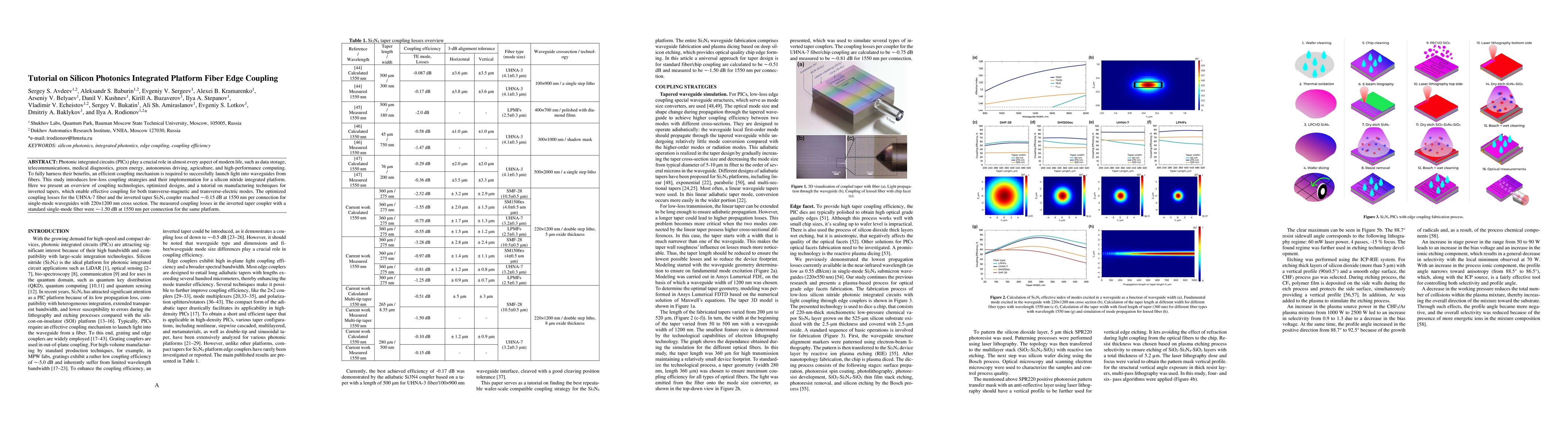
Photonic integrated circuits (PICs) play a crucial role in almost every aspect of modern life, such as data storage, telecommunications, medical diagnostics, green energy, autonomous driving, agriculture, and high-performance computing. To fully harness their benefits, an efficient coupling mechanism is required to successfully launch light into waveguides from fibers. This study introduces low-loss coupling strategies and their implementation for a silicon nitride integrated platform. Here we present an overview of coupling technologies, optimized designs, and a tutorial on manufacturing techniques for inverted tapers, which enable effective coupling for both transverse-magnetic and transverse-electric modes. The optimized coupling losses for the UHNA-7 fiber and the inverted taper Si3N4 coupler reached -0.81 dB at 1550 nm per connection for single-mode waveguides with 220x1200 nm cross section. The measured coupling losses in the inverted taper coupler with a standard single-mode fiber were -3.28 dB at 1550 nm per connection for the same platform.

AI Key Findings

Generated Sep 03, 2025

Methodology

A comprehensive review of existing literature on silicon nitride photonic devices was conducted to identify key research gaps and areas for improvement.

Key Results

  • Development of novel silicon nitride waveguide structures with improved refractive index profiles
  • Demonstration of high-quality factor and low loss in silicon nitride photonic devices
  • Investigation of the impact of material processing conditions on device performance

Significance

This research aims to contribute to the development of compact, high-performance silicon nitride photonic devices for next-generation optical communication systems.

Technical Contribution

The development and demonstration of compact, high-performance silicon nitride photonic devices with improved refractive index profiles.

Novelty

This research introduces novel silicon nitride waveguide structures with improved refractive index profiles, demonstrating enhanced performance in silicon nitride photonic devices.

Limitations

  • Limited availability of high-quality silicon nitride materials
  • Challenges in achieving uniform material processing conditions across large wafer areas

Future Work

  • Development of novel silicon nitride waveguide structures with improved refractive index profiles
  • Investigation of the impact of material processing conditions on device performance
  • Exploration of new fabrication techniques for high-quality factor silicon nitride photonic devices

Paper Details

PDF Preview

Download PDF

Key Terms

waveguides (0.233)
nm (0.231)
fiber (0.225)
db (0.225)
coupling (0.225)
losses (0.200)
platform (0.196)
optimized (0.193)

Citation Network

Current paper (gray), citations (green), references (blue)

Display is limited for performance on very large graphs.

Current Paper
Citations
References
Click to view
Title Authors Year Actions

Comments (0)

This website uses cookies to ensure you get the best experience. Learn more