Quick Summary:

This paper presents a method for creating two-dimensional covalent crystals by chemically converting van der Waals materials, specifically converting exfoliated indium selenide (InSe) to indium fluoride (InF3) through direct fluorination. The resulting InF3 layers exhibit semiconductor properties with a direct bandgap of 2.2 eV, demonstrating scalability and potential for synthesizing diverse novel atomically thin covalent crystals.

Summary

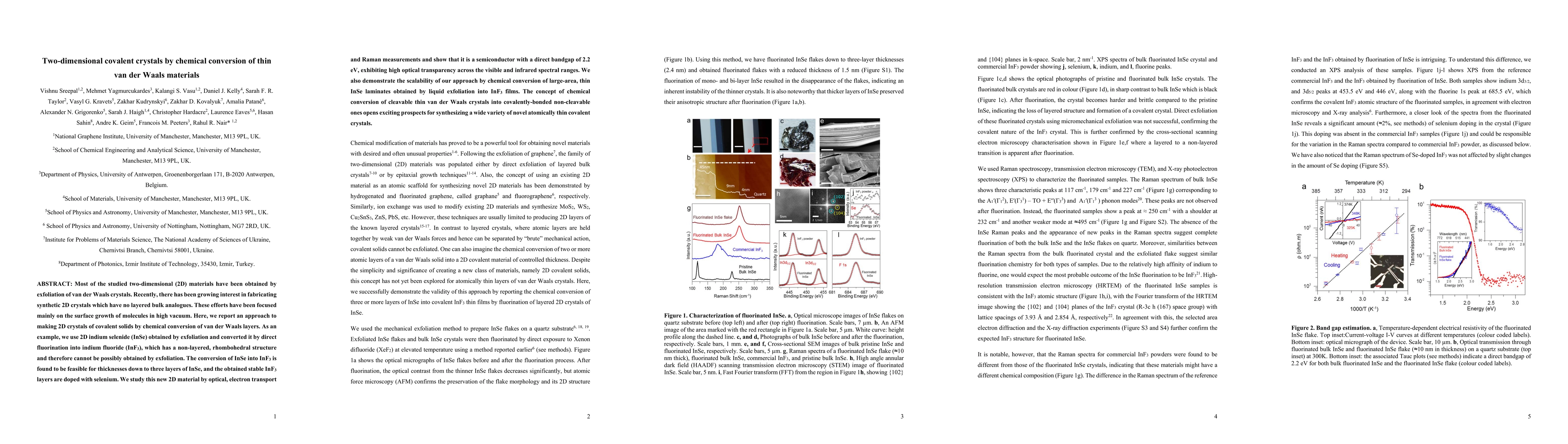
Most of the studied two-dimensional (2D) materials have been obtained by exfoliation of van der Waals crystals. Recently, there has been growing interest in fabricating synthetic 2D crystals which have no layered bulk analogues. These efforts have been focused mainly on the surface growth of molecules in high vacuum. Here, we report an approach to making 2D crystals of covalent solids by chemical conversion of van der Waals layers. As an example, we use 2D indium selenide (InSe) obtained by exfoliation and converted it by direct fluorination into indium fluoride (InF3), which has a non-layered, rhombohedral structure and therefore cannot be possibly obtained by exfoliation. The conversion of InSe into InF3 is found to be feasible for thicknesses down to three layers of InSe, and the obtained stable InF3 layers are doped with selenium. We study this new 2D material by optical, electron transport and Raman measurements and show that it is a semiconductor with a direct bandgap of 2.2 eV, exhibiting high optical transparency across the visible and infrared spectral ranges. We also demonstrate the scalability of our approach by chemical conversion of large-area, thin InSe laminates obtained by liquid exfoliation into InF3 films. The concept of chemical conversion of cleavable thin van der Waals crystals into covalently-bonded non-cleavable ones opens exciting prospects for synthesizing a wide variety of novel atomically thin covalent crystals.

AI Key Findings

Get AI-generated insights about this paper's methodology, results, and significance.

Paper Details

PDF Preview

Download PDF

Key Terms

crystals (0.307)
der (0.277)
conversion (0.276)
van (0.262)
layers (0.204)
chemical (0.202)
layered (0.201)
obtained (0.169)
direct (0.144)
optical (0.134)
solids (0.131)
raman (0.131)
exhibiting (0.123)
opens (0.120)
semiconductor (0.118)
doped (0.117)
ranges (0.116)
ev (0.115)
prospects (0.114)
efforts (0.114)

Citation Network

Current paper (gray), citations (green), references (blue)

Current Paper
Citations
References
Click to view
Title Authors Year Actions
Downscaling of Non-Van der Waals Semimetallic W5N6 with Resistivity Preservation.
Hongze Gao, D. Zhou, Lu Ping, Zifan Wang, N. T. Hung, Jun Cao, M. Geiwitz, Gabriel Natale, Y. Lin, K. Burch, Riichiro Saito, Mauricio Terrones, Xi Ling
2025
View Paper
Advancing Nanoelectronics Applications: Progress in Non-van der Waals 2D Materials.
Hongze Gao, Zifan Wang, Jun Cao, Y. Lin, X. Ling
2024
View Paper
Calculation of the energy of a two-dimensional hydrogen molecule
Nataliia Kashirina, Y. Kashyrina, O. Korol, O. Roik
2023
View Paper
In Situ Assembly of Well-Defined MoS2 Slabs on Shape-Tailored Anatase TiO2 Nanostructures: Heterojunctions Role in Phenol Photodegradation
Rosangela Santalucia, Paolo Negro, T. Vacca, F. Pellegrino, A. Damin, F. Cesano, D. Scarano
2022
View Paper
Experimental and DFT studies of selenium decorated graphene oxide: Redox stability, cytotoxicity, and corrosion inhibition of AZ13 Mg alloy
P. N, I. Cole, A. Kuznetsov, K. Thomas, P. Ruszkowski, M. Kujawska
2022
View Paper
Non-van der Waals quasi-2D materials; recent advances in synthesis, emergent properties and applications
A. Balan, Anand B. Puthirath, Soumyabrata Roy, G. Costin, E. Oliveira, M. Saadi, V. Sreepal, Rico Friedrich, Peter Serles, Abhijit Biswas, Sathvik Ajay Iyengar, Nithya Chakingal, S. Bhattacharyya, Sreehari K. Saju, Samuel Castro Pardo, Lucas M. Sassi, T. Filleter, A. Krasheninnikov, D. Galvão, R. Vajtai, R. Nair, P. Ajayan
2022
View Paper
Morphotaxy of Layered van der Waals Materials.
David Lam, Dmitry Lebedev, M. Hersam
2022
View Paper
High-throughput assessment of two-dimensional electrode materials for energy storage devices
Arnab Kabiraj, S. Mahapatra
2022
View Paper
Adjusting crystal morphology and emission behavior of organic fluorophore via the synergistic effect of proton and anion
Guigui Ye, Yinhe Qu, Lina Su, Yingzhong Li, Baozhu Chi, Hongming Wang, G. Xia
2021
View Paper
Enhanced properties of covalently coupled borophene-graphene layers through fluorination and hydrogenation
A. Kochaev, R. Meftakhutdinov, R. Sibatov, K. Katin, M. Maslov, V. Efimov
2021
View Paper
2D materials inks toward smart flexible electronics
O. A. Moses, Libo Gao, Haitao Zhao, Zhuo Wang, Mukhtar Lawan Adam, Zhehao Sun, Kaili Liu, Jiahong Wang, Yang Lu, Z. Yin, Xue‐Feng Yu
2021
View Paper
Vibrational and optical identification of GeO2 and GeO single layers: a first-principles study.
Y. Sozen, M. Yagmurcukardes, H. Sahin
2021
View Paper
A structure map for AB2 type 2D materials using high-throughput DFT calculations
M. Fukuda, Jingning Zhang, Yung-Ting Lee, T. Ozaki
2021
View Paper
Tunable electronic and optical properties of InSe/arsenene heterostructure by vertical strain and electric field
X. Deng, Q. Jing
2021
View Paper
Surface functionalization of the honeycomb structure of zinc antimonide (ZnSb) monolayer: A first-Principles study
A. Bafekry, M. Shahrokhi, M. Yagmurcukardes, D. Gogova, M. Ghergherehchi, B. Akgenc, S. Feghhi
2021
View Paper
Bandgap engineering of layered mono-chalcogenides via pressure
Heqi Xiong, Ruiping Li, Yingchun Cheng, G. Xing, Wei Huang
2021
View Paper
Ultra-thin structures of manganese fluorides: conversion from manganese dichalcogenides by fluorination.
M. Baskurt, R. Nair, F. Peeters, H. Sahin
2021
View Paper
Interface Confinement in Metal Nanosheet for High-Efficiency Semi-Hydrogenation of Alkynes
Chenqi Shen, Yujin Ji, Pengtang Wang, Shuxing Bai, Man Wang, Youyong Li, Xiaoqing Huang, Qi Shao
2021
View Paper
Theoretical insight into two-dimensional g-C6N6/InSe van der Waals Heterostructure: A promising visible-light photocatalyst
Junli Chang, Ning Dong, Guangzhao Wang, Liping Jiang, Hongkuan Yuan, Hong Chen
2021
View Paper
Electro-optical and mechanical properties of Zinc antimonide (ZnSb) monolayer and bilayer: A first-principles study
A. Bafekry, M. Yagmurcukardes, M. Shahrokhi, M. Ghergherehchi, D. Kim, B. Mortazavi
2021
View Paper
Stable Janus TaSe2 single-layers via surface functionalization
Z. Kahraman, M. Baskurt, M. Yagmurcukardes, A. Chaves, H. Sahin
2021
View Paper
Few-Layered MoS2 Nanoparticles Covering Anatase TiO2 Nanosheets: Comparison between Ex Situ and In Situ Synthesis Approaches
Rosangela Santalucia, T. Vacca, F. Cesano, G. Martra, F. Pellegrino, D. Scarano
2020
View Paper
Tunable electronic properties of the dynamically stable layered mineral Pt2HgSe3 (Jacutingaite).
A. Bafekry, C. Stampfl, C. Nguyen, M. Ghergherehchi, B. Mortazavi
2020
View Paper
Enhanced photoresponse and fast charge transfer: three-dimensional macroporous g-C3N4/GO-TiO2 nanostructure for hydrogen evolution
Wei Li, Qiong Ma, Xiao Wang, Xiao-shan Chu, Feixin Wang, Xue-chuan Wang, Chuan-yi Wang
2020
View Paper
Composition formula of transparent conductive tin doped indium oxide in terms of cluster plus glue atom model
Hao Liu, Yi Zhang, Xin Zhang, Quan Wang, Hualin Wang, Shuang Zhang, Yanping Ma, Yunxian Cui, W. Ding, C. Dong
2020
View Paper
Non-layered 2D materials toward advanced photoelectric devices: progress and prospects
Zhaoqiang Zheng, Jiandong Yao, Jingbo Li, Guowei Yang
2020
View Paper
Ultrastrong adhesion of fluorinated graphene on a substrate: In situ electrochemical conversion to ionic-covalent bonding at the interface
Yu-Yu Sin, Cheng-Chun Huang, Cin-Nan Lin, Jui-Kung Chih, Y. Hsieh, I. Tsao, Ju Li, C. Su
2020
View Paper
Two-dimensional materials for energy conversion and storage
Hengcong Tao, Qun Fan, T. Ma, Shizhen Liu, H. Gysling, J. Texter, Fen Guo, Zhenyu Sun
2020
View Paper
Interlayer Bonding in Two-Dimensional Materials: The Special Case of SnP3 and GeP3.
A. Slassi, S. M. Gali, A. Pershin, Á. Gali, J. Cornil, D. Beljonne
2020
View Paper
High-throughput discovery of high Curie point two-dimensional ferromagnetic materials
Arnab Kabiraj, Mayank Kumar, S. Mahapatra
2020
View Paper
Functionalization of single-layer TaS_2 and formation of ultrathin Janus structures
Z. Kahraman, M. Yagmurcukardes, H. Sahin
2020
View Paper
Flexible N doped carbon/bubble-like MoS2 core/sheath framework: Buffering volume expansion for potassium ion batteries.
G. Suo, Jiaqi Zhang, Dan Li, Qiyao Yu, M. He, Lei Feng, Xiaojiang Hou, Yanling Yang, Xiaohui Ye, Li Zhang, Wen Wang
2020
View Paper
Raman and optical characteristics of van der Waals heterostructures of single layers of GaP and GaSe: a first-principles study
Y. Sozen, H. Sahin
2021
View Paper
Interlayer engineering of MoS2 nanosheets for high-rate potassium-ion storage
W. Kang, Yuchen Wang, Cuihua An
2020
View Paper
author-version of: Two-dimensional heterostructures formed by graphenelike ZnO and MgO monolayers for optoelectronic applications
Mahsa Seyedmohammadzadeh, C. Sevik, O˘guz G¨ulseren
View Paper

Comments (0)

This website uses cookies to ensure you get the best experience. Learn more