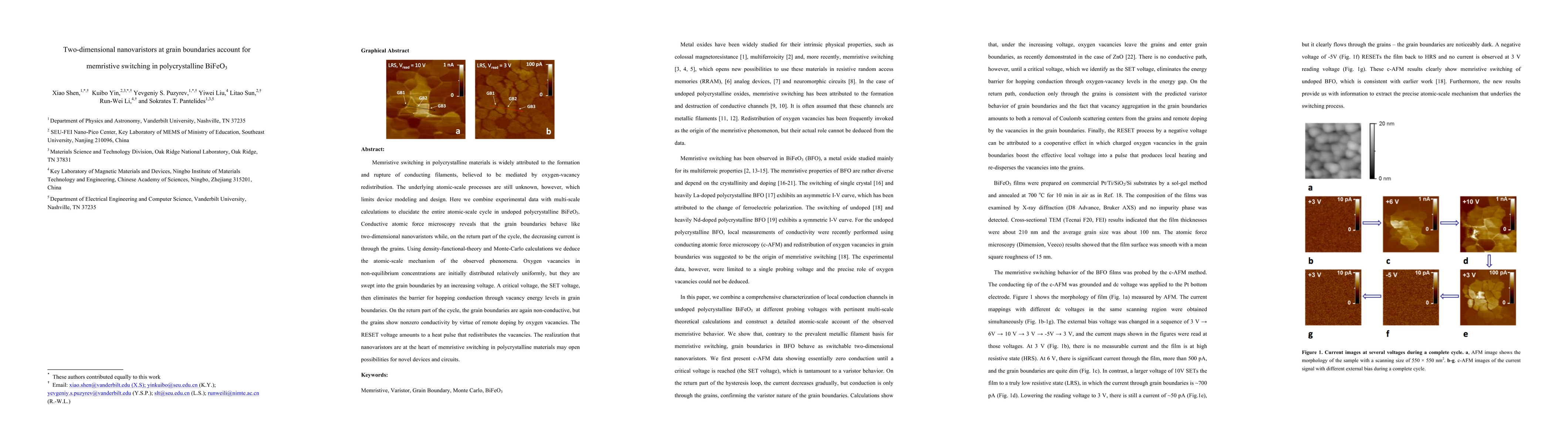
This paper reveals that grain boundaries in polycrystalline BiFeO3 act as two-dimensional nanovaristors, driving memristive switching through oxygen-vacancy redistribution. The study combines experimental and computational methods to show that the SET voltage creates conductive pathways via grain boundary vacancies, while the RESET voltage redistributes these vacancies, leading to novel device design possibilities.
Memristive switching in polycrystalline materials is widely attributed to the formation and rupture of conducting filaments, believed to be mediated by oxygen-vacancy redistribution. The underlying atomic-scale processes are still unknown, however, which limits device modeling and design. Here we combine experimental data with multi-scale calculations to elucidate the entire atomic-scale cycle in undoped polycrystalline BiFeO3. Conductive atomic force microscopy reveals that the grain boundaries behave like two-dimensional nanovaristors while, on the return part of the cycle, the decreasing current is through the grains. Using density-functional-theory and Monte-Carlo calculations we deduce the atomic-scale mechanism of the observed phenomena. Oxygen vacancies in non-equilibrium concentrations are initially distributed relatively uniformly, but they are swept into the grain boundaries by an increasing voltage. A critical voltage, the SET voltage, then eliminates the barrier for hopping conduction through vacancy energy levels in grain boundaries. On the return part of the cycle, the grain boundaries are again non-conductive, but the grains show nonzero conductivity by virtue of remote doping by oxygen vacancies. The RESET voltage amounts to a heat pulse that redistributes the vacancies. The realization that nanovaristors are at the heart of memristive switching in polycrystalline materials may open possibilities for novel devices and circuits.
This graph shows how this paper is connected to other research. The current paper is shown in dark gray, papers that cite it are in green, and papers it references are in blue. You can:
• Hover over any node to see the paper title
• Click a node to view that paper's details
• Drag nodes to rearrange the graph
• Use the zoom controls (bottom right) to zoom in/out
Title | Authors | Year | Actions |
---|---|---|---|
Ferroelectric State in an α-Nd2WO6 Polymorph Stabilized in a Thin Film
|
T. Carlier, M. Chambrier, A. Da Costa, Florent Blanchard, T. Denneulin, M. Letiche, P. Roussel, R. Desfeux, A. Ferri
|
2020
|
View Paper |
Electronic mechanism for resistive switching in metal/insulator/metal nanodevices
|
H. Raebiger, A. C. Padilha, Alexandre Reily Reily Rocha, G. Dalpian
|
2020
|
View Paper |
Progress in BiFeO3-based heterostructures: materials, properties and applications.
|
Li Yin, W. Mi
|
2019
|
View Paper |
Tip Induced Surface Defect migration and Conductivity Studies in Tetragonal, Rhombohedral and Mixed-Phase epitaxial BiFeO_3 Thin Films
|
M. M. Saj Mohan, M. Sreenath, Ranjith Ramadurai
|
2018
|
View Paper |
Microstructure and local electrical behavior in [(Nd2Ti2O7)4/(SrTiO3)n]10 (n = 4–8) superlattices
|
T. Carlier, A. Ferri, S. Saitzek, M. Huvé, A. Bayart, A. Da Costa, R. Desfeux, A. Tebano
|
2018
|
View Paper |
Memristive devices from ZnO nanowire bundles and meshes
|
Y. Puzyrev, Xiao Shen, C. X. Zhang, J. Hachtel, K. Ni, B. Choi, E. Zhang, O. Ovchinnikov, peixiong zhao, D. Fleetwood, S. Pantelides
|
2017
|
View Paper |
Visible‐Light Driven Nanoscale Photoconductivity of Grain Boundaries in Self‐Supported ZnO Nano‐ and Microstructured Platelets
|
N. Faraji, C. Ulrich, N. Wolff, L. Kienle, R. Adelung, Y. Mishra, J. Seidel
|
2016
|
View Paper |
Highly Itinerant Atomic Vacancies in Phosphorene.
|
Yongqing Cai, Qingqing Ke, Gang Zhang, B. Yakobson, Yong‐Wei Zhang
|
2016
|
View Paper |
Roles of grain boundary and oxygen vacancies in Ba 0.6 Sr 0.4 TiO 3 films for resistive switching device application
|
Xiaobing Yan, J. Zhao, Y. Li, Yucheng Li, Zhenyu Zhou, Yuanyuan Zhang
|
2016
|
View Paper |
Roles of grain boundary and oxygen vacancies in Ba0.6Sr0.4TiO3 films for resistive switching device application
|
X. B. Yan, J. Zhao, Y. Li, Y. Li, Z. Zhou, Y. Y. Zhang
|
2016
|
View Paper |
Resistive Switching in Nanodevices
|
H. Raebiger, A. C. Padilha, A. Rocha, G. Dalpian
|
2015
|
View Paper |
High On/Off Ratio Memristive Switching of Manganite/Cuprate Bilayer by Interfacial Magnetoelectricity
|
Xiao Shen, T. Pennycook, D. Hernandez-Martin, A. P'erez, M. Varela, Y. Puzyrev, C. León, Z. Sefrioui, J. Santamaria, S. Pantelides
|
2015
|
View Paper |
Proceedings of the 2 nd NanoWorld Conference in Boston ( NWC-2017 ) . Part III : Featured Presentations
|
C. S. Lee, Hyungsub Kim, Dahyun Choi, Kwangmin Kim, Minji Lee, W. Chu, D. Chun, S. Ahn
|
2017
|
View Paper |
Published: 2019-06-12
Comments (0)