Ultra-high mobility semiconducting epitaxial graphene on silicon carbide
Publication
Metrics
AI Quick Summary
This paper demonstrates a quasi-equilibrium annealing method that produces highly ordered epitaxial graphene on silicon carbide with a 0.6 eV bandgap and ultra-high mobility exceeding 5000 cm²/Vs, making it a promising material for advanced nanoelectronics applications. The graphene is robust, aligned with the SiC substrate, and can be conventionally patterned.
Paper Preview
Abstract
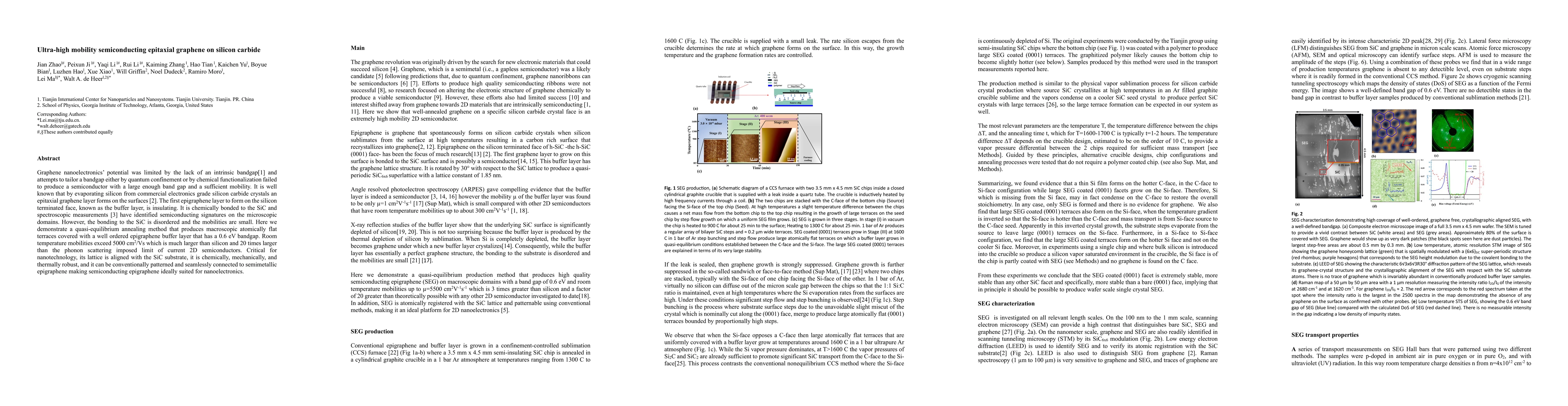
Graphene nanoelectronics potential was limited by the lack of an intrinsic bandgap[1] and attempts to tailor a bandgap either by quantum confinement or by chemical functionalization failed to produce a semiconductor with a large enough band gap and a sufficient mobility. It is well known that by evaporating silicon from commercial electronics grade silicon carbide crystals an epitaxial graphene layer forms on the surfaces [2]. The first epigraphene layer to form on the silicon terminated face, known as the buffer layer, is insulating. It is chemically bonded to the SiC and spectroscopic measurements [3] have identified semiconducting signatures on the microscopic domains. However, the bonding to the SiC is disordered and the mobilities are small. Here we demonstrate a quasi-equilibrium annealing method that produces macroscopic atomically flat terraces covered with a well ordered epigraphene buffer layer that has a 0.6 eV bandgap. Room temperature mobilities exceed 5000 cm2/Vs which is much larger than silicon and 20 times larger than the phonon scattering imposed limit of current 2D semiconductors. Critical for nanotechnology, its lattice is aligned with the SiC substrate, it is chemically, mechanically, and thermally robust, and it can be conventionally patterned and seamlessly connected to semimetallic epigraphene making semiconducting epigraphene ideally suited for nanoelectronics.
AI Key Findings
Get AI-generated insights about this paper's methodology, results, significance, and more — seven facets brought into focus.
Impact
Paper Details
Authors
PDF Preview
Key Terms
Citation Network
Current paper (gray), citations (green), references (blue)
Display is limited for performance on very large graphs.
Discussion 0