Publication
Metrics
Paper Preview
Abstract
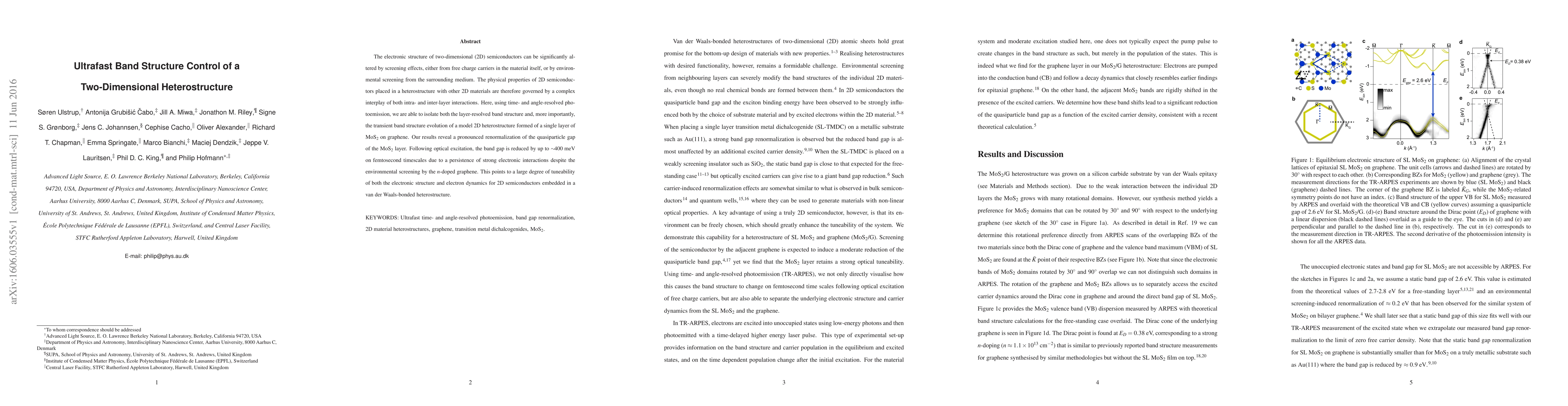
The electronic structure of two-dimensional (2D) semiconductors can be significantly altered by screening effects, either from free charge carriers in the material itself, or by environmental screening from the surrounding medium. The physical properties of 2D semiconductors placed in a heterostructure with other 2D materials are therefore governed by a complex interplay of both intra- and inter-layer interactions. Here, using time- and angle-resolved photoemission, we are able to isolate both the layer-resolved band structure and, more importantly, the transient band structure evolution of a model 2D heterostructure formed of a single layer of MoS$_2$ on graphene. Our results reveal a pronounced renormalization of the quasiparticle gap of the MoS$_2$ layer. Following optical excitation, the band gap is reduced by up to $\sim\!$400 meV on femtosecond timescales due to a persistence of strong electronic interactions despite the environmental screening by the $n$-doped graphene. This points to a large degree of tuneability of both the electronic structure and electron dynamics for 2D semiconductors embedded in a van der Waals-bonded heterostructure.
AI Key Findings
Get AI-generated insights about this paper's methodology, results, significance, and more — seven facets brought into focus.
Impact
Paper Details
PDF Preview
Key Terms
Citation Network
Current paper (gray), citations (green), references (blue)
Display is limited for performance on very large graphs.
Discussion 0