All-dielectric nanoantennas are a promising alternative to plasmonic optical
antennas for engineering light emission because of their low-loss nature in the
optical spectrum. Nevertheless, it is still challenging to manipulate
directional light emission with subwavelength all-dielectric nanoantennas.
Here, we propose and numerically demonstrate that a hollow silicon nanodisk can
serve as a versatile antenna for directing and enhancing the emission from
either an electric or magnetic dipole emitter. When primarily coupled to both
electric and magnetic dipole modes of a nanoantenna, broadband
nearly-unidirectional emission can be realized by the interference of two
modes, which can be spectrally tuned via the geometric parameters in an easy
way. More importantly, the emission directions for the magnetic and electric
dipole emitters are shown as opposite to each other through control of the
phase difference between the induced magnetic and electric dipole modes of the
antenna. Meanwhile, the Purcell factors can be enhanced by more than one order
of magnitude and high quantum efficiencies can be maintained at the visible
spectrum for both kinds of dipole emitters. We further show that these
unidirectional emission phenomena can withstand small disorder effects of
in-plane dipole orientation and location. Our study provides a simple yet
versatile platform that can shape the emission of both magnetic and electric
dipole emitters.
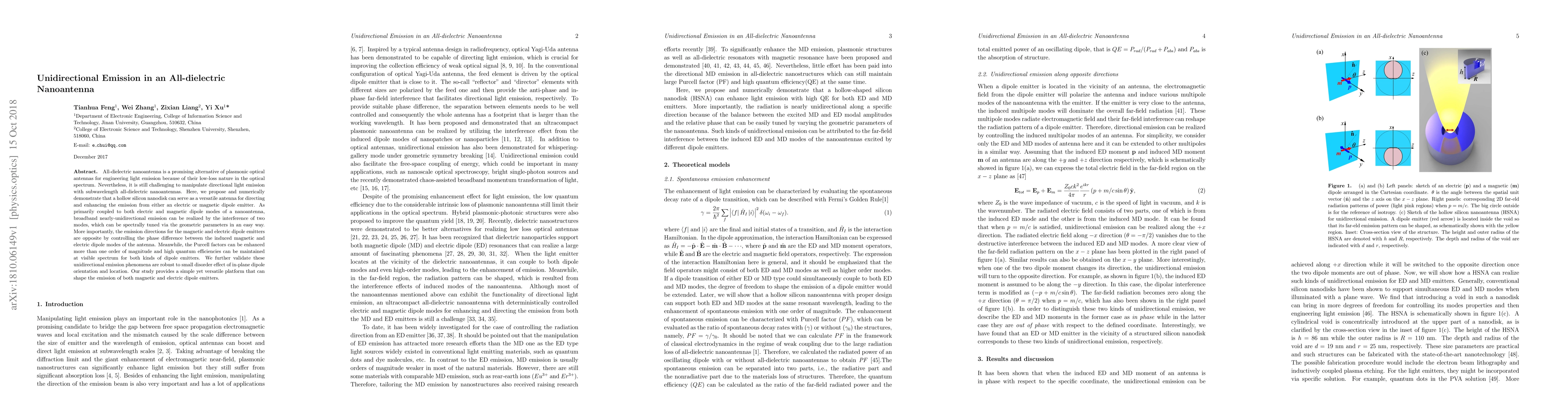
Discussion 0