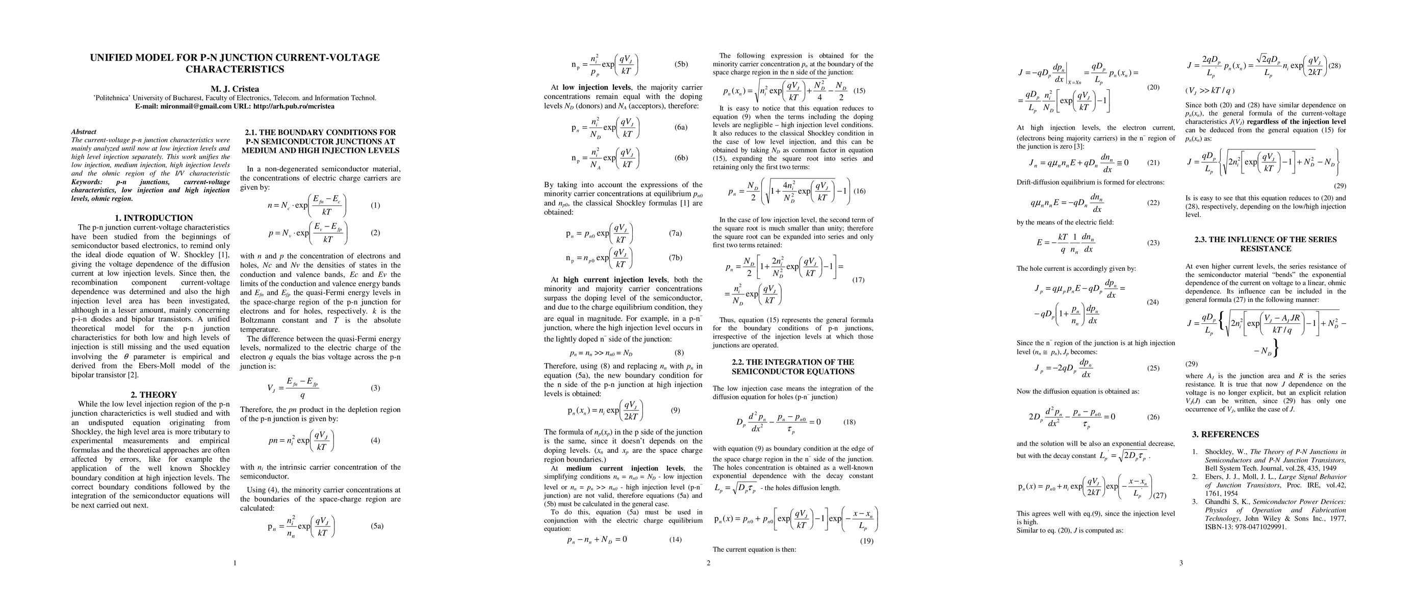
This paper presents a unified model that integrates the current-voltage characteristics of p-n junctions across low, medium, and high injection levels, as well as the ohmic region. The study aims to provide a comprehensive analysis of the I/V characteristics under various injection conditions.
The current-voltage p-n junction characteristics were mainly analyzed until now at low injection levels and high level injection separately. This work unifies the low injection, medium injection, high injection levels and the ohmic region of the I/V characteristics. Keywords: p-n junctions, current-voltage characteristics, low injection and high injection levels, ohmic region.
Get AI-generated insights about this paper's methodology, results, and significance.
Current paper (gray), citations (green), references (blue)
Title | Authors | Year | Actions |
---|---|---|---|
Shallow Si N + P junction diodes realized via molecular monolayer doping
|
Astha Tapriya, Brian Novak, Scott A. Williams, S. Kurinec
|
2018
|
View Paper |
Heavy and light hole minority carrier transport properties in low-doped n-InGaAs lattice matched to InP
|
A. Walker, M. Denhoff
|
2017
|
View Paper |
Fractional Interpretation of Anomalous Diffusion and Semiconductor Equations
|
Rohith G., Ajayan K.K.
|
2012
|
View Paper |
Diamond membranes for photonic devices
|
Kerem Bray, Blake Regan, I. Aharonovich
|
2021
|
View Paper |
Dual-Axis Solar Tracker Without Microcontroller
|
Sohom Chakraborty, A. Roy, Sukanya Dey
|
2021
|
View Paper |
Ultra-Shallow Phosphorous Diffusion in Silicon using Molecular Monolayer Doping
|
Astha Tapriya
|
2017
|
View Paper |
Comments (0)