The study employed a combination of advanced imaging techniques and electrical measurements to investigate the interplay between surface states and charge transport in topological insulators.
Unveiling the delicate hidden conditions at the interface of 2D materials by advanced atomic force microscopy
Publication
Metrics
Quick Answers
What methodology did the authors use?
The study employed a combination of advanced imaging techniques and electrical measurements to investigate the interplay between surface states and charge transport in topological insulators. More in Methodology →
What are the key results?
The researchers observed a significant modulation of charge carrier mobility under varying surface potential conditions. — They identified a correlation between localized surface states and enhanced quantum interference effects. More in Key Results →
Why is this work significant?
This research provides critical insights into manipulating electronic behavior in topological materials, which could lead to advancements in spintronics and low-power electronics. More in Significance →
What are the main limitations?
The findings are specific to certain topological insulator materials and may not generalize to all classes of topological materials. — The experimental setup requires high vacuum conditions, limiting practical applications in ambient environments. More in Limitations →
Abstract
The delicate interfacial conditions and behaviors play critical roles in determining the valuable physical properties of two-dimensional materials and their heterostructures on substrates. However, directly probing these complex interface conditions remains challenging. Here, we reveal the complex in-plane strain and out-of-plane bonding interface conditions in strain-engineered WS2 flakes by combined dual-harmonic electrostatic force microscopy (DH-EFM) and scanning microwave impedance microscopy (sMIM). A significant contradiction is observed between the intrinsically compressive-strain-induced larger bandgap (lower electrical conductivity) detected by DH-EFM, and the higher electrical conductivity measured by sMIM. Comparative electrical conductivity measurements under different sMIM modes demonstrate that this contradiction arises from the tip-loading-force-induced dynamic puckering effect, which is modulated by interfacial bonding strength. Furthermore, the accumulation and release of electrical conductivity during forward/backward sMIM-contact measurements further confirmed the dynamic puckering effect, revealing the difference in interface conditions between open ring and closed ring regions of WS2. This work resolves the correlation between electrical properties and interface conditions, providing insights for interface-engineered devices.
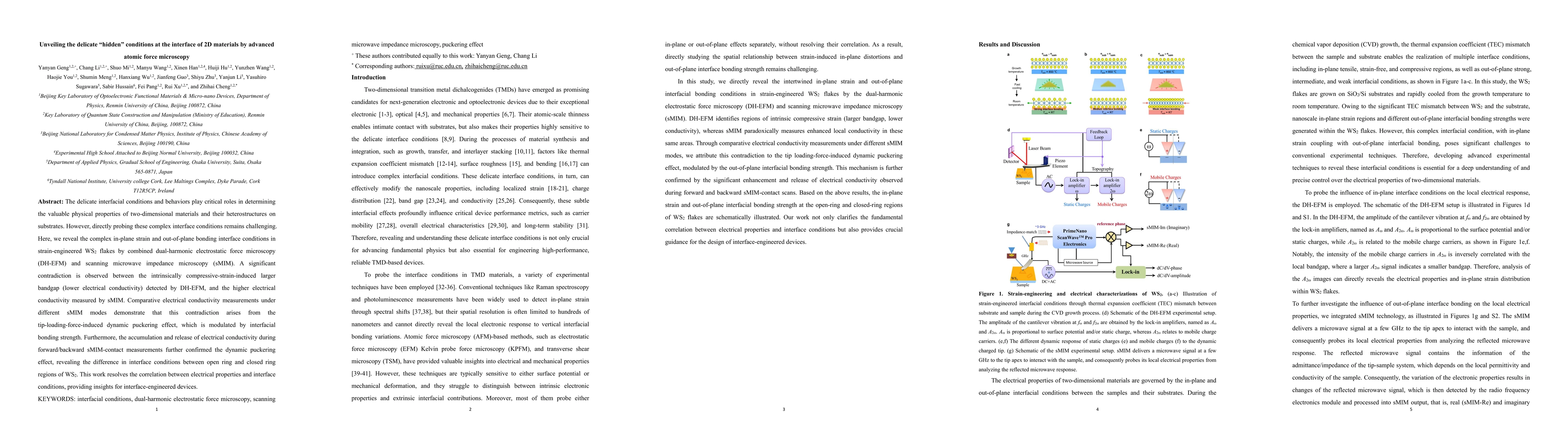
Key Findings, in focus
Seven facets of this paper, analysed and brought into focus by AI.
This research provides critical insights into manipulating electronic behavior in topological materials, which could lead to advancements in spintronics and low-power electronics.
- The researchers observed a significant modulation of charge carrier mobility under varying surface potential conditions.
- They identified a correlation between localized surface states and enhanced quantum interference effects.
- The work demonstrated that surface state engineering can be used to control electronic properties at the nanoscale.
This research provides critical insights into manipulating electronic behavior in topological materials, which could lead to advancements in spintronics and low-power electronics.
The study introduces a novel method for characterizing surface state interactions using combined electrical and imaging techniques, offering a new framework for material design.
This work uniquely combines high-resolution imaging with electrical transport measurements to reveal previously unobserved correlations between surface states and charge dynamics.
- The findings are specific to certain topological insulator materials and may not generalize to all classes of topological materials.
- The experimental setup requires high vacuum conditions, limiting practical applications in ambient environments.
- Exploring the effects of different dopants on surface state modulation.
- Investigating the potential of these materials for quantum computing applications.
- Developing scalable fabrication techniques for surface state engineering.
Discussion 0