Summary
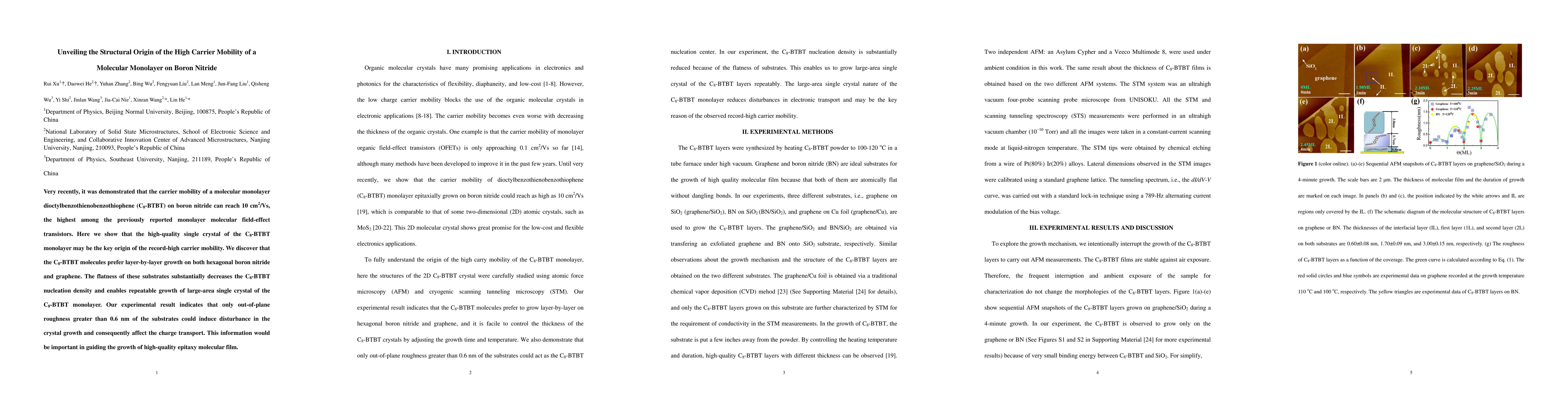
Very recently, it was demonstrated that the carrier mobility of a molecular monolayer dioctylbenzothienobenzothiophene (C8-BTBT) on boron nitride can reach 10 cm2/Vs, the highest among the previously reported monolayer molecular field-effect transistors. Here we show that the high-quality single crystal of the C8-BTBT monolayer may be the key origin of the record-high carrier mobility. We discover that the C8-BTBT molecules prefer layer-by-layer growth on both hexagonal boron nitride and graphene. The flatness of these substrates substantially decreases the C8-BTBT nucleation density and enables repeatable growth of large-area single crystal of the C8-BTBT monolayer. Our experimental result indicates that only out-of-plane roughness greater than 0.6 nm of the substrates could induce disturbance in the crystal growth and consequently affect the charge transport. This information would be important in guiding the growth of high-quality epitaxy molecular film.
AI Key Findings
Get AI-generated insights about this paper's methodology, results, and significance.
Paper Details
PDF Preview
Key Terms
Citation Network
Current paper (gray), citations (green), references (blue)
Display is limited for performance on very large graphs.
| Title | Authors | Year | Actions |
|---|
Comments (0)