ArxivLens

Publication

Published: Apr 08, 2026
Categories: physics.optics

Metrics

Source: ArXiv

Quick Answers

What methodology did the authors use?

Integrated a deep‑UV (250 nm) LED co‑illumination module into a JEOL 7001 SEM with precise lateral, axial, and tilt control; incorporated a linear wire‑grid polarizer for s‑polarized light; performed electrical feedthrough design and FDTD simulations to predict E‑field enhancement at dielectric interfaces. More in Methodology →

What are the key results?

Successful implementation of UV‑C co‑illumination that enhances normal E‑field (Ez) at dielectric interfaces, increasing secondary electron yield without metal coating. — FDTD simulations confirm significant field enhancement at nanostructures (e.g., graphite on diamond, Si/SiO₂) and predict improved imaging contrast for low‑conductivity samples. More in Key Results →

Why is this work significant?

Provides a non‑destructive, high‑contrast imaging modality for low‑conductivity and nanostructured materials, enabling work‑function mapping and characterization of 2D materials and high‑entropy alloys without sample coating. More in Significance →

What are the main limitations?

UV intensity limited by LED power and duty cycle, restricting maximum secondary electron yield. — Current system supports only s‑polarized illumination; p‑polarization and full azimuthal control are not yet implemented. More in Limitations →

Paper Preview

Abstract

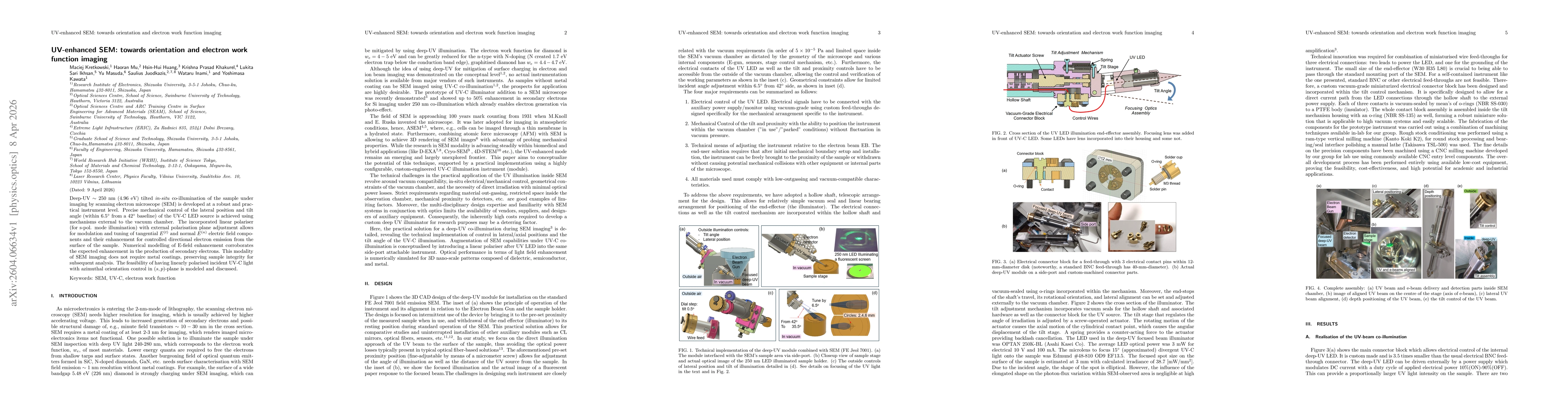
Deep-UV ~ 250 nm (4.96 eV) tilted in-situ co-illumination of the sample under imaging by scanning electron microscope (SEM) is developed at a robust and practical instrument level. Precise mechanical control of the lateral position and tilt angle (within 6.5$^\circ$ from a 42$^\circ$ baseline) of the UV-C LED source is achieved using mechanisms external to the vacuum chamber. The incorporated linear polariser (for s-pol. mode illumination) with external polarisation plane adjustment allows for modulation and tuning of tangential $E^{(t)}$ and normal $E^{(n)}$ electric field components and their enhancement for controlled directional electron emission from the surface of the sample. Numerical modelling of E-field enhancement corroborates the expected enhancement in the production of secondary electrons. This modality of SEM imaging does not require metal coatings, preserving sample integrity for subsequent analysis. The feasibility of having linearly polarised incident UV-C light with azimuthal orientation control in $(s,p)$-plane is modeled and discussed.

Key Findings, in focus

Seven facets of this paper, analysed and brought into focus by AI.

AI-generated · verify against source Generated Apr 09, 2026
In focus · one-line synthesis

Provides a non‑destructive, high‑contrast imaging modality for low‑conductivity and nanostructured materials, enabling work‑function mapping and characterization of 2D materials and high‑entropy alloys without sample coating.

01
MethodologyHow they did it

Integrated a deep‑UV (250 nm) LED co‑illumination module into a JEOL 7001 SEM with precise lateral, axial, and tilt control; incorporated a linear wire‑grid polarizer for s‑polarized light; performed electrical feedthrough design and FDTD simulations to predict E‑field enhancement at dielectric interfaces.

02
ResultsWhat they found
  • Successful implementation of UV‑C co‑illumination that enhances normal E‑field (Ez) at dielectric interfaces, increasing secondary electron yield without metal coating.
  • FDTD simulations confirm significant field enhancement at nanostructures (e.g., graphite on diamond, Si/SiO₂) and predict improved imaging contrast for low‑conductivity samples.
  • Demonstrated that s‑polarized UV illumination at ~250 nm produces directional photoemission, enabling potential work‑function imaging and high‑resolution SEM of 2D materials.
03
SignificanceWhy it matters

Provides a non‑destructive, high‑contrast imaging modality for low‑conductivity and nanostructured materials, enabling work‑function mapping and characterization of 2D materials and high‑entropy alloys without sample coating.

04
Technical ContributionsWhat's new technically

Compact, vacuum‑compatible UV‑C co‑illumination module with precise mechanical control and integrated electrical feedthrough, enabling directional photoemission in SEM.

05
NoveltyWhat sets it apart

First demonstration of linear‑polarized UV‑C co‑illumination in SEM to enhance secondary electron emission via field enhancement, without metal coating, guided by FDTD modeling.

06
LimitationsWhat to be cautious about
  • UV intensity limited by LED power and duty cycle, restricting maximum secondary electron yield.
  • Current system supports only s‑polarized illumination; p‑polarization and full azimuthal control are not yet implemented.
07
Future WorkWhere it goes next
  • Implement a rotating polarizer to enable p‑polarized and arbitrary azimuthal UV illumination, enhancing Ez further.
  • Integrate multi‑wavelength UV sources and combine with other SEM techniques (EDS, EELS) for comprehensive material analysis.

Paper Details

Paper ID: 2604.06634
Comments: Under review at Advanced Photonics Research
Categories:
physics.optics

How to Cite This Paper

Reference manager: RIS EndNote


Discussion 0

This website uses cookies to ensure you get the best experience. Learn more