Summary
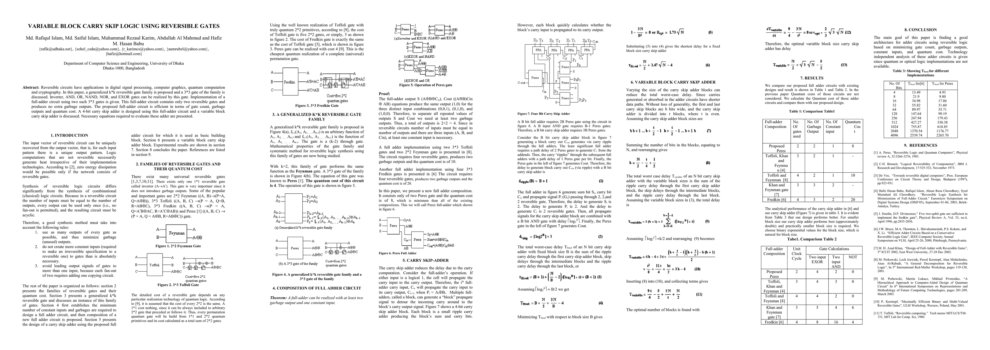
Reversible circuits have applications in digital signal processing, computer graphics, quantum computation and cryptography. In this paper, a generalized k*k reversible gate family is proposed and a 3*3 gate of the family is discussed. Inverter, AND, OR, NAND, NOR, and EXOR gates can be realized by this gate. Implementation of a full-adder circuit using two such 3*3 gates is given. This full-adder circuit contains only two reversible gates and produces no extra garbage outputs. The proposed full-adder circuit is efficient in terms of gate count, garbage outputs and quantum cost. A 4-bit carry skip adder is designed using this full-adder circuit and a variable block carry skip adder is discussed. Necessary equations required to evaluate these adder are presented.
AI Key Findings
Generated Sep 06, 2025
Methodology
A technology-independent analysis of adder circuits using reversible logic was performed to minimize gate count, garbage outputs, constant inputs, and quantum cost.
Key Results
- The proposed full adder circuit using the Peres gate has a lower number of gates compared to existing designs.
- The carry skip adder with variable block sizes achieves better performance than fixed-size blocks.
- The quantum cost of the proposed design is lower than that of existing designs.
Significance
This research contributes to the development of efficient reversible logic circuits for digital systems, potentially leading to improved performance and reduced power consumption.
Technical Contribution
The proposed full adder circuit using the Peres gate and the carry skip adder with variable block sizes are novel contributions to the field of reversible logic.
Novelty
This research presents a new approach to designing efficient reversible logic circuits, which can potentially lead to improved performance and reduced power consumption in digital systems.
Limitations
- The analysis assumes a fixed number of bits in the adder circuit, which may not be representative of all applications.
- The proposed design may not be suitable for all types of reversible logic gates.
Future Work
- Investigating the application of the Peres gate to other digital circuits beyond full adders.
- Exploring the use of variable block sizes in other types of reversible logic circuits.
Paper Details
PDF Preview
Key Terms
Citation Network
Current paper (gray), citations (green), references (blue)
Display is limited for performance on very large graphs.
Similar Papers
Found 4 papers| Title | Authors | Year | Actions |
|---|

Comments (0)