This paper reports high-performance electronic devices based on a vertical van der Waals heterostructure of WSe2/SnSe2, achieving a high current on-off ratio and ultra-high rectification ratio due to effective modulation of charge carrier transport and energy barriers. The demonstrated small signal half-wave rectifier circuit indicates potential for future high-speed electronic applications.
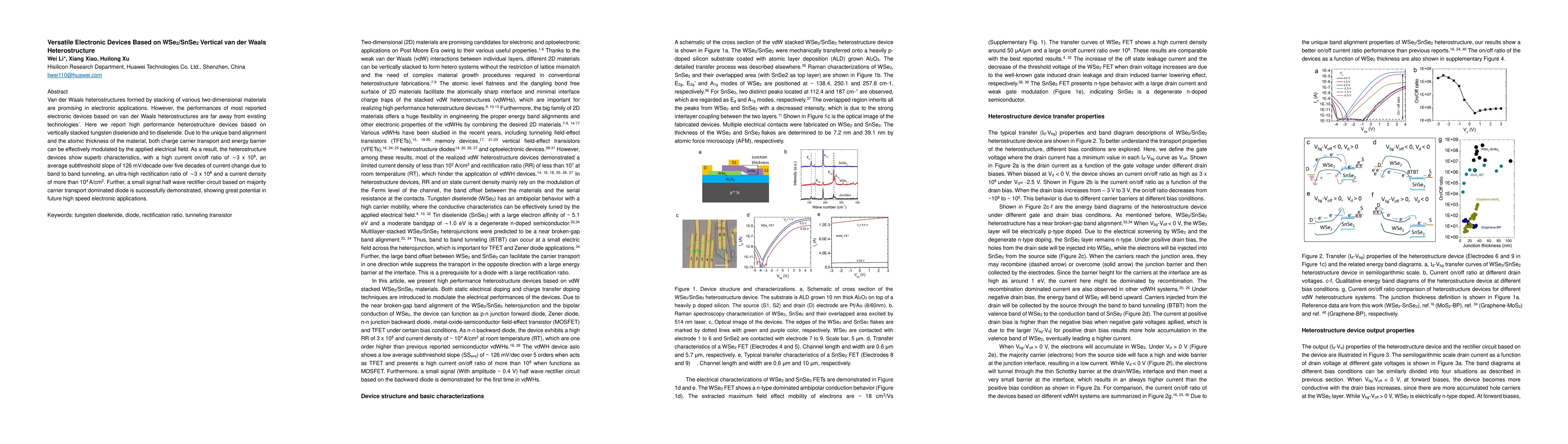
Van der Waals heterostructures formed by stacking of various two-dimensional materials are promising in electronic applications. However, the performances of most reported electronic devices based on van der Waals heterostructures are far away from existing technologies'. Here we report high performance heterostructure devices based on vertically stacked tungsten diselenide and tin diselenide. Due to the unique band alignment and the atomic thickness of the material, both charge carrier transport and energy barrier can be effectively modulated by the applied electrical field. As a result, the heterostructure devices show superb characteristics, with a high current on-off ratio of around 3 x 10⁸, an average subthreshold slope of 126 mV per decade over five decades of current change due to band to band tunneling, an ultra-high rectification ratio of around 3 x 10⁸ and a current density of more than 104 A per cm2. Further, a small signal half wave rectifier circuit based on majority carrier transport dominated diode is successfully demonstrated, showing great potential in future high speed electronic applications.
Get AI-generated insights about this paper's methodology, results, and significance.
Current paper (gray), citations (green), references (blue)
Xiaodong Xu, Zhaoyu Liu, Yuzhou Zhao et al.
Title | Authors | Year | Actions |
---|---|---|---|
High Hole Mobility van der Waals Junction Field-Effect Transistors Based on Te/GaAs for Multimode Photodetection and Logic Applications.
|
Fei Li, Jiang Zeng, Yiming Zhao, Lingyu Zhu, Yao Zhou, Zuyi Wang, Zhen Wang, Yuhang Zhang, Guoxin Liu, J. Xiong, Wei Gao, Mengmeng Yang, Jingbo Li, Nengjie Huo, Yiming Sun
|
2025
|
View Paper |
Simulation of Optoelectronic Synaptic Behavior in SnSe2/WSe2 Heterojunction Transistors
|
Zixuan Huang, Lisheng Wang, Yifan Zhang, Zhenpeng Cheng, Fengxiang Chen
|
2025
|
View Paper |
Investigating the Electrical Transport and Photoresponse Properties of WSe2 and a Thermally Engineered SrTiO3-Based Heterojunction
|
A. Arora, Parvesh Chander, Akshay Tomar, Sonika Kodan, Ramesh Chandra, V. K. Malik
|
2024
|
View Paper |
Tunable Electronic Properties and Contact Performance of Type‐II HfS2${\rm HfS}_2$/MoS2${\rm MoS}_2$ Van der Waals Heterostructure
|
Son-Tung Nguyen, Nguyen V. Hieu, H. Le-Quoc, Kien Nguyen-Ba, C. V. Nguyen, Cuong Q. Nguyen
|
2024
|
View Paper |
Single-Gate MoS2 Tunnel FET with a Thickness-Modulated Homojunction.
|
Tomohiro Fukui, Tomonori Nishimura, Yasumitsu Miyata, Keiji Ueno, T. Taniguchi, Kenji Watanabe, K. Nagashio
|
2024
|
View Paper |
Theoretical insight on the effect of middle layer specifications on electronic properties of SnS2/MX2/SnS2 Trilayer heterostructure (M = Mo, w; X = S, Se, Te)
|
A. Tiwari, Arunabh Singh, Naresh Bahadursha, Subhajit Das, Sudipta Chakraborty, S. Kanungo
|
2024
|
View Paper |
Ferroelectric gating of two-dimensional semiconductors for the integration of steep-slope logic and neuromorphic devices
|
S. Kamaei, Xia Liu, A. Saeidi, Ying Wei, C. Gastaldi, J. Brugger, A. Ionescu
|
2023
|
View Paper |
Atomically Thin Twisted Heterostructure Optoelectronics Enhanced via vdW Interface Engineering
|
Lingshan Li, Xiang Fu, Liang Zhang, S. Ullah, X. Gao, Yixiu Wang, Wenzhuo Wu, Yuan Xiang, Qing Yang
|
2023
|
View Paper |
Electrically Self-Aligned, Reconfigurable Test Structure Using WSe2/SnSe2 Heterojunction for TFET and MOSFET
|
P. Dasika, Kenji Watanabe, T. Taniguchi, K. Majumdar
|
2022
|
View Paper |
Few‐layered MoS2 Based Vertical van der Waals p‐n Homojunction by Highly‐efficient N2 Plasma Implantation
|
Yufeng Shan, Ziwei Yin, Jiaqi Zhu, Xin Li, Wei Dou, Yue Wang, Chi-Lun Liu, H. Deng, N. Dai
|
2022
|
View Paper |
Strong interfacial coupling in vertical WSe2/WS2 heterostructure for high performance photodetection
|
Wenxia You, B. Zheng, Zheyuan Xu, Ying Jiang, Chenguang Zhu, Weihao Zheng, Xin Yang, Xingxia Sun, Jieyuan Liang, Xiao Yi, Tinghao Wang, Fei Gao, Xiaoli Zhu, Quan Yuan, Dong Li, A. Pan
|
2022
|
View Paper |
Intrinsic Electronic Transport Properties and Carrier Densities in PtS2 and SnSe2: Exploration of n+‐Source for 2D Tunnel FETs
|
Yuichiro Sato, T. Nishimura, Duanfei Dong, K. Ueno, K. Shinokita, K. Matsuda, K. Nagashio
|
2021
|
View Paper |
Reconfigurable Tunneling Transistors Heterostructured by an Individual Carbon Nanotube and MoS2.
|
Gaotian Lu, Yang Wei, Xuanzhang Li, G. Zhang, Guang Wang, Liang Liang, Qunqing Li, S. Fan, Yuegang Zhang
|
2021
|
View Paper |
Emerging Opportunities for Electrostatic Control in Atomically Thin Devices.
|
M. Beck, M. Hersam
|
2020
|
View Paper |
Comments (0)