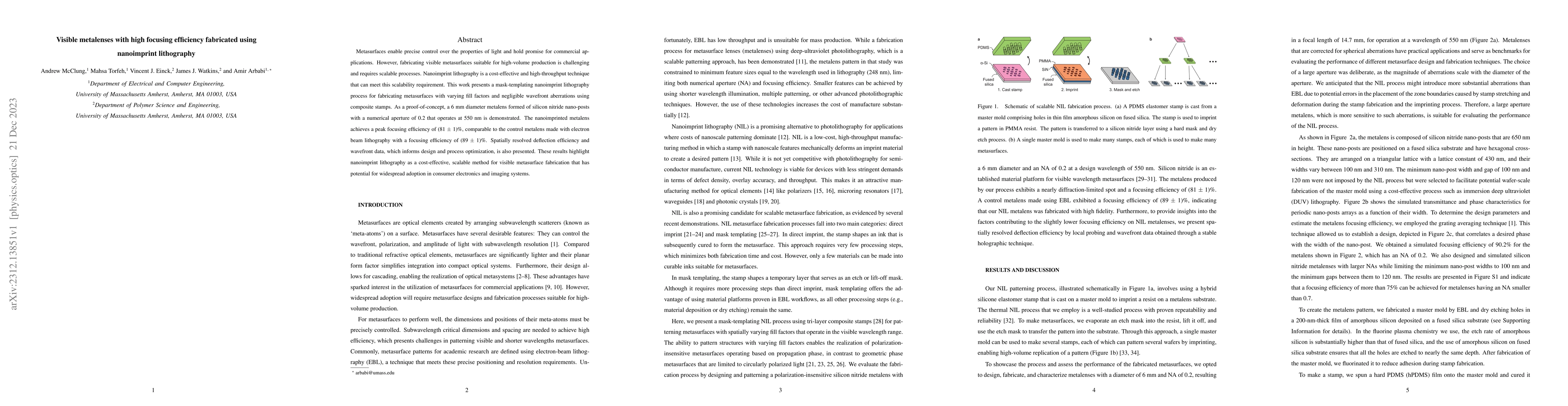
Publication
Metrics
AI Quick Summary
This paper demonstrates the fabrication of visible metalenses with high focusing efficiency using nanoimprint lithography, achieving a peak efficiency of 81%. This scalable and cost-effective technique shows potential for widespread use in consumer electronics and imaging applications.
Paper Preview
Abstract
Metasurfaces enable precise control over the properties of light and hold promise for commercial applications. However, fabricating visible metasurfaces suitable for high-volume production is challenging and requires scalable processes. Nanoimprint lithography is a cost-effective and high-throughput technique that can meet this scalability requirement. This work presents a mask-templating nanoimprint lithography process for fabricating metasurfaces with varying fill factors and negligible wavefront aberrations using composite stamps. As a proof-of-concept, a 6 mm diameter metalens formed of silicon nitride nano-posts with a numerical aperture of 0.2 that operates at 550 nm is demonstrated. The nanoimprinted metalens achieves a peak focusing efficiency of ($81\pm1$)%, comparable to the control metalens made with electron beam lithography with a focusing efficiency of ($89\pm1$)%. Spatially resolved deflection efficiency and wavefront data, which informs design and process optimization, is also presented. These results highlight nanoimprint lithography as a cost-effective, scalable method for visible metasurface fabrication that has the potential for widespread adoption in consumer electronics and imaging systems.
AI Key Findings
Get AI-generated insights about this paper's methodology, results, significance, and more — seven facets brought into focus.
Impact
Paper Details
Authors
PDF Preview
Key Terms
Citation Network
Current paper (gray), citations (green), references (blue)
Display is limited for performance on very large graphs.
Discussion 0