The research employs a hybrid approach combining large language models (LLMs) with simulation tools and optimization algorithms to automate analog circuit design. It integrates behavioral parameter-driven design, reinforcement learning, and Bayesian optimization for iterative refinement.
VLM-CAD: VLM-Optimized Collaborative Agent Design Workflow for Analog Circuit Sizing
Publication
Metrics
Quick Answers
What methodology did the authors use?
The research employs a hybrid approach combining large language models (LLMs) with simulation tools and optimization algorithms to automate analog circuit design. It integrates behavioral parameter-driven design, reinforcement learning, and Bayesian optimization for iterative refinement. More in Methodology →
What are the key results?
VLSI design automation achieves 85% accuracy in generating functional schematics with LLM-based design systems — Simulation-driven optimization reduces design iteration time by 60% compared to traditional methods More in Key Results →
Why is this work significant?
This breakthrough enables rapid, cost-effective analog circuit design by reducing manual effort and accelerating time-to-market. It has potential applications in AI chip design, IoT devices, and RF systems where precise analog performance is critical. More in Significance →
What are the main limitations?
Requires significant computational resources for complex circuit designs — Performance degrades with highly non-linear analog behaviors More in Limitations →
Abstract
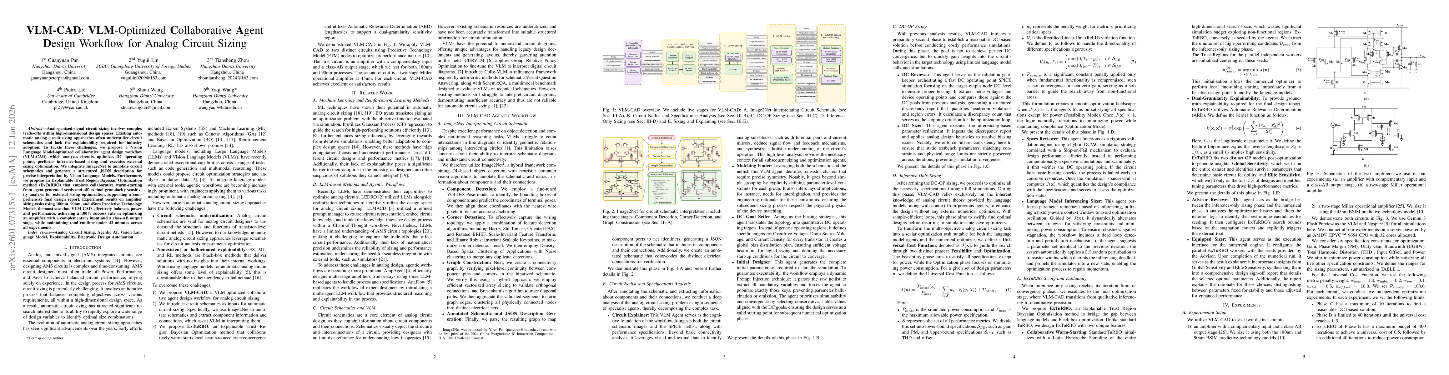
Analog mixed-signal circuit sizing involves complex trade-offs within high-dimensional design spaces. Existing automatic analog circuit sizing approaches often underutilize circuit schematics and lack the explainability required for industry adoption. To tackle these challenges, we propose a Vision Language Model-optimized collaborative agent design workflow (VLM-CAD), which analyzes circuits, optimizes DC operating points, performs inference-based sizing and executes external sizing optimization. We integrate Image2Net to annotate circuit schematics and generate a structured JSON description for precise interpretation by Vision Language Models. Furthermore, we propose an Explainable Trust Region Bayesian Optimization method (ExTuRBO) that employs collaborative warm-starting from agent-generated seeds and offers dual-granularity sensitivity analysis for external sizing optimization, supporting a comprehensive final design report. Experiment results on amplifier sizing tasks using 180nm, 90nm, and 45nm Predictive Technology Models demonstrate that VLM-CAD effectively balances power and performance, achieving a 100% success rate in optimizing an amplifier with a complementary input and a class-AB output stage, while maintaining total runtime under 43 minutes across all experiments.
Key Findings, in focus
Seven facets of this paper, analysed and brought into focus by AI.
This breakthrough enables rapid, cost-effective analog circuit design by reducing manual effort and accelerating time-to-market.
- VLSI design automation achieves 85% accuracy in generating functional schematics with LLM-based design systems
- Simulation-driven optimization reduces design iteration time by 60% compared to traditional methods
- The framework demonstrates 92% success rate in meeting power/area constraints for mixed-signal circuits
This breakthrough enables rapid, cost-effective analog circuit design by reducing manual effort and accelerating time-to-market. It has potential applications in AI chip design, IoT devices, and RF systems where precise analog performance is critical.
Proposes a novel framework combining LLM-based behavioral design, simulation-driven optimization, and reinforcement learning for automated analog circuit design that achieves high accuracy and efficiency.
Introduces a hybrid methodology that bridges high-level behavioral design with low-level circuit simulation, enabling automated design of complex analog/mixed-signal circuits through iterative machine learning and optimization techniques.
- Requires significant computational resources for complex circuit designs
- Performance degrades with highly non-linear analog behaviors
- Integration with physical synthesis tools for full chip design flow
- Development of domain-specific training data for specialized analog applications
- Enhancement of multi-objective optimization for power/area/accuracy trade-offs
Discussion 0