Summary
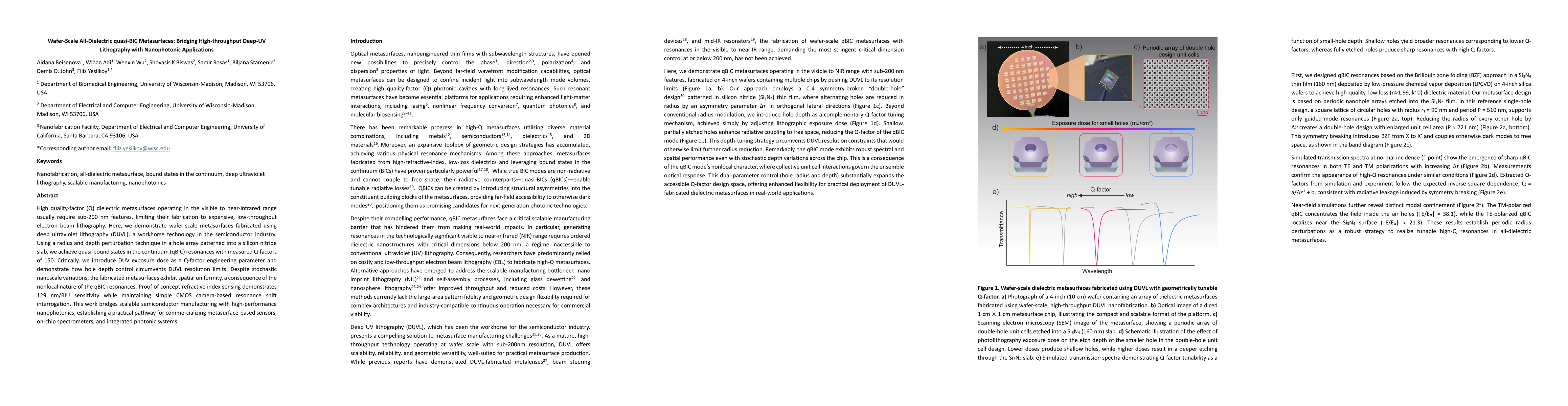
High quality-factor (Q) dielectric metasurfaces operating in the visible to near-infrared range usually require sub-200 nm features, limiting their fabrication to expensive, low-throughput electron beam lithography. Here, we demonstrate wafer-scale metasurfaces fabricated using deep ultraviolet lithography (DUVL), a workhorse technology in the semiconductor industry. Using a radius and depth perturbation technique in a hole array patterned into a silicon nitride slab, we achieve quasi-bound states in the continuum (qBIC) resonances with measured Q-factors of 150. Critically, we introduce DUV exposure dose as a Q-factor engineering parameter and demonstrate how hole depth control circumvents DUVL resolution limits. Despite stochastic nanoscale variations, the fabricated metasurfaces exhibit spatial uniformity, a consequence of the nonlocal nature of the qBIC resonances. Proof of concept refractive index sensing demonstrates 129 nm/RIU sensitivity while maintaining simple CMOS camera-based resonance shift interrogation. This work bridges scalable semiconductor manufacturing with high-performance nanophotonics, establishing a practical pathway for commercializing metasurface-based sensors, on-chip spectrometers, and integrated photonic systems.
AI Key Findings
Generated Oct 21, 2025
Methodology
The research employs deep ultraviolet lithography (DUVL) to fabricate wafer-scale all-dielectric metasurfaces with sub-200 nm features. They use radius and depth perturbation techniques in a hole array patterned into a silicon nitride slab to achieve quasi-BIC resonances. DUV exposure dose is controlled as a parameter to engineer Q-factors, and the fabricated metasurfaces are characterized using hyperspectral imaging and refractive index sensing experiments.
Key Results
- Achieved quasi-BIC resonances with Q-factors of 150 using DUVL
- Demonstrated 129 nm/RIU refractive index sensitivity with CMOS camera-based interrogation
- Observed spatial uniformity in qBIC resonances despite stochastic nanoscale variations
Significance
This work bridges scalable semiconductor manufacturing with high-performance nanophotonics, enabling commercialization of metasurface-based sensors, on-chip spectrometers, and integrated photonic systems. It provides a practical pathway for mass-producing high-Q dielectric metasurfaces with nanoscale features.
Technical Contribution
Introduction of DUV exposure dose as a Q-factor engineering parameter in DUVL-fabricated metasurfaces, enabling precise control over qBIC resonance properties.
Novelty
First demonstration of wafer-scale all-dielectric quasi-BIC metasurfaces fabricated using DUVL, combining high-throughput semiconductor manufacturing with nanophotonic functionality through exposure dose-controlled hole depth and occupancy.
Limitations
- Spectral undersampling limits detection of ultra-high Q factors at higher doses
- Stochastic nanoscale variations may affect performance in some applications
Future Work
- Exploring optimization of DUV exposure parameters for even higher Q-factors
- Investigating integration with CMOS systems for real-time sensing applications
- Developing advanced fabrication techniques for complex metasurface designs
Paper Details
PDF Preview
Similar Papers
Found 5 papersReconfigurable, Temperature Resilient Phase-Change Metasurfaces Fabricated via High Throughput Nanoimprinting Lithography
Jose Santiso, Agustin Mihi, Carlota Ruiz de Galarreta et al.
Enhanced second harmonic generation in high-$Q$ all-dielectric metasurfaces with backward frequency conversion
Feng Wu, Jiajun Li, Tingting Liu et al.
Optofluidic transport and particle trapping using an all-dielectric quasi-BIC metasurface
Sen Yang, Justus C. Ndukaife
Robust enhancement of high-harmonic generation from all-dielectric metasurfaces enabled by polarization-insensitive bound states in the continuum
Tingting Liu, Shuyuan Xiao, Meibao Qin et al.
Comments (0)