Wafer-Scale Squeezed-Light Chips

Source: ArXiv
Share: Share on X LinkedIn

Summary

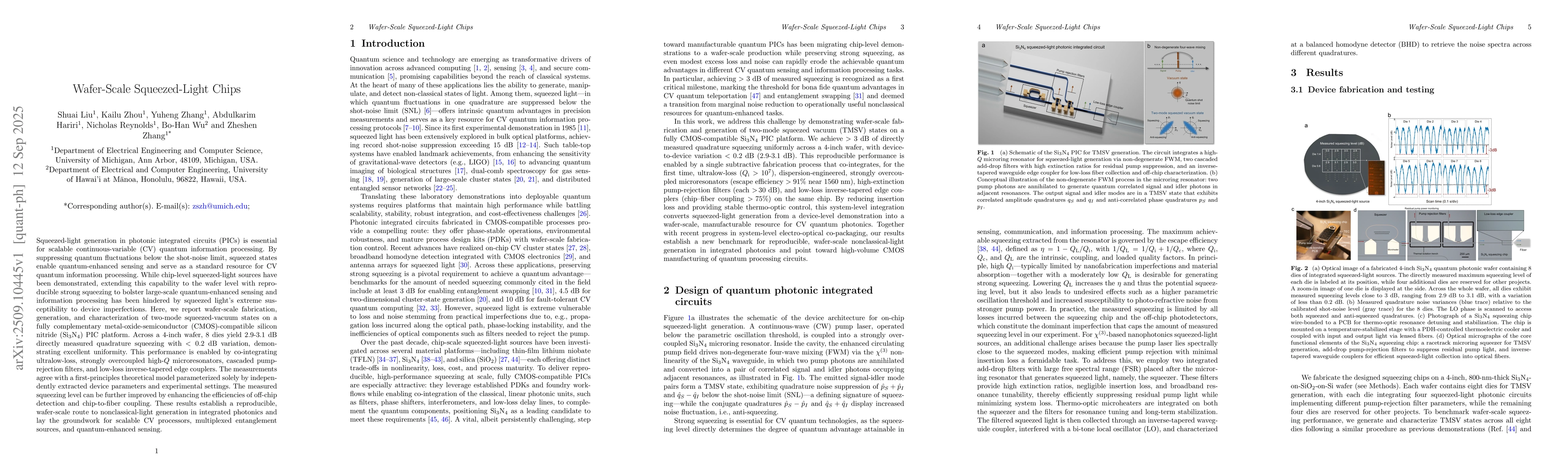
Squeezed-light generation in photonic integrated circuits (PICs) is essential for scalable continuous-variable (CV) quantum information processing. By suppressing quantum fluctuations below the shot-noise limit, squeezed states enable quantum-enhanced sensing and serve as a standard resource for CV quantum information processing. While chip-level squeezed-light sources have been demonstrated, extending this capability to the wafer level with reproducible strong squeezing to bolster large-scale quantum-enhanced sensing and information processing has been hindered by squeezed light's extreme susceptibility to device imperfections. Here, we report wafer-scale fabrication, generation, and characterization of two-mode squeezed-vacuum states on a fully complementary metal-oxide-semiconductor (CMOS)-compatible silicon nitride (Si$_3$N$_4$) PIC platform. Across a 4-inch wafer, 8 dies yield 2.9-3.1 dB directly measured quadrature squeezing with $< 0.2$ dB variation, demonstrating excellent uniformity. This performance is enabled by co-integrating ultralow-loss, strongly overcoupled high-$Q$ microresonators, cascaded pump-rejection filters, and low-loss inverse-tapered edge couplers. The measurements agree with a first-principles theoretical model parameterized solely by independently extracted device parameters and experimental settings. The measured squeezing level can be further improved by enhancing the efficiencies of off-chip detection and chip-to-fiber coupling. These results establish a reproducible, wafer-scale route to nonclassical-light generation in integrated photonics and lay the groundwork for scalable CV processors, multiplexed entanglement sources, and quantum-enhanced sensing.

AI Key Findings

Generated Oct 17, 2025

Methodology

The study employs a wafer-scale fabrication process for silicon nitride photonic integrated circuits, utilizing electron-beam lithography and inductively coupled plasma reactive ion etching to create microresonators and waveguides. Quantum characterization is performed using balanced homodyne detection with a tunable laser and polarization controllers, while classical characterization involves Lorentzian fitting of resonance spectra to extract quality factors.

Key Results

  • Achieved wafer-scale fabrication of ultra-low-loss silicon nitride photonic chips with dispersion-engineered waveguides
  • Demonstrated quantum squeezing of light with a depth exceeding 3.5 dB in a Kerr microresonator
  • Enabled stable and reproducible operation of microheater-based thermal tuning for on-chip devices

Significance

This research advances integrated quantum photonics by demonstrating scalable fabrication techniques and high-quality quantum light sources, which are critical for developing compact quantum communication and computing systems.

Technical Contribution

Development of a wafer-scale fabrication process for silicon nitride photonic circuits with dispersion engineering and integration of microheaters for thermal tuning, enabling scalable quantum photonic devices.

Novelty

The work presents the first demonstration of wafer-scale quantum photonic integrated circuits with simultaneous achievement of ultra-low loss, dispersion engineering, and active thermal tuning for quantum light sources.

Limitations

  • Current fabrication process may have yield limitations at wafer scale
  • Thermal tuning requires precise control of microheater temperatures

Future Work

  • Optimize fabrication process to improve yield and reduce defects
  • Explore integration of nonlinear optical components for enhanced quantum functionality
  • Investigate hybrid quantum systems combining photonic and superconducting circuits

Paper Details

PDF Preview

Download PDF

Similar Papers

Found 4 papers

Comments (0)

This website uses cookies to ensure you get the best experience. Learn more