WaferSegClassNet is a lightweight AI-based computer vision network designed for simultaneous classification and segmentation of semiconductor wafer defects. It uses a shared encoder for efficient end-to-end training and achieves high accuracy with minimal computational resources, significantly outperforming previous models.
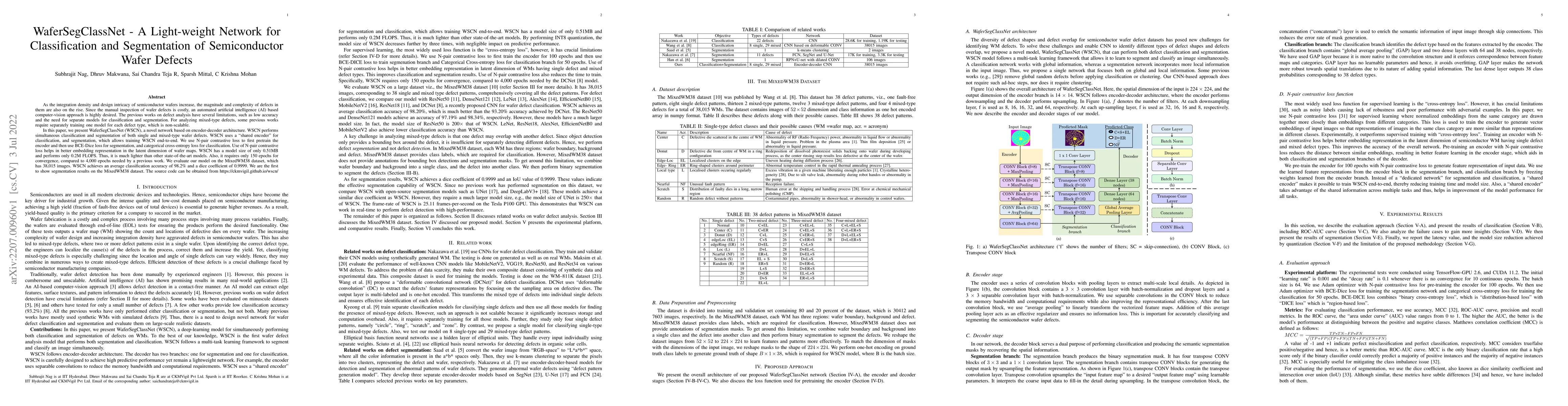
As the integration density and design intricacy of semiconductor wafers increase, the magnitude and complexity of defects in them are also on the rise. Since the manual inspection of wafer defects is costly, an automated artificial intelligence (AI) based computer-vision approach is highly desired. The previous works on defect analysis have several limitations, such as low accuracy and the need for separate models for classification and segmentation. For analyzing mixed-type defects, some previous works require separately training one model for each defect type, which is non-scalable. In this paper, we present WaferSegClassNet (WSCN), a novel network based on encoder-decoder architecture. WSCN performs simultaneous classification and segmentation of both single and mixed-type wafer defects. WSCN uses a "shared encoder" for classification, and segmentation, which allows training WSCN end-to-end. We use N-pair contrastive loss to first pretrain the encoder and then use BCE-Dice loss for segmentation, and categorical cross-entropy loss for classification. Use of N-pair contrastive loss helps in better embedding representation in the latent dimension of wafer maps. WSCN has a model size of only 0.51MB and performs only 0.2M FLOPS. Thus, it is much lighter than other state-of-the-art models. Also, it requires only 150 epochs for convergence, compared to 4,000 epochs needed by a previous work. We evaluate our model on the MixedWM38 dataset, which has 38,015 images. WSCN achieves an average classification accuracy of 98.2% and a dice coefficient of 0.9999. We are the first to show segmentation results on the MixedWM38 dataset. The source code can be obtained from https://github.com/ckmvigil/WaferSegClassNet.
This graph shows how this paper is connected to other research. The current paper is shown in dark gray, papers that cite it are in green, and papers it references are in blue. You can:
• Hover over any node to see the paper title
• Click a node to view that paper's details
• Drag nodes to rearrange the graph
• Use the zoom controls (bottom right) to zoom in/out
Title | Authors | Year | Actions |
---|---|---|---|
Frequency-domain multi-scale Kolmogorov-Arnold representation attention network for mixed-type wafer defect recognition
|
Qihang Huang, Fan Zhang, Yuqian Zhao, Ji’an Duan
|
2025
|
View Paper |
SEM-CLIP: Precise Few-Shot Learning for Nanoscale Defect Detection in Scanning Electron Microscope Image
|
Qian Jin, Yuqi Jiang, Xudong Lu, Yumeng Liu, Yining Chen, Dawei Gao, Qi Sun, Cheng Zhuo
|
2025
|
View Paper |
Contrastive Learning with Global and Local Representation for Mixed-Type Wafer Defect Recognition
|
Shantong Yin, Yangkun Zhang, Rui Wang
|
2025
|
View Paper |
YOLOSeg with applications to wafer die particle defect segmentation
|
Yen-Ting Li, Yu-Cheng Chan, Chen-Che Huang, Yu-Chang Hsu, Ssu-Han Chen
|
2025
|
View Paper |
Enhanced detection of unknown defect patterns on wafer bin maps based on an open-set recognition approach
|
Jin-Su Shin, Min-Joo Kim, Beom-Seok Kim, Dong-Hee Lee
|
2025
|
View Paper |
A depthwise convolutional neural network model based on active contour for multi-defect wafer map pattern classification
|
Jeonghoon Choi, Dongjun Suh
|
2025
|
View Paper |
Global feature identification layer for mixed-type wafer bin map classification
|
Jaehyeon Joo, Chang-Ouk Kim
|
2025
|
View Paper |
WCDenseNet:An efficient wafermap classification method based on DenseNet
|
Shuyang Xu, Zeguang Wang
|
2024
|
View Paper |
YOLOv8-seg-CP: a lightweight instance segmentation algorithm for chip pad based on improved YOLOv8-seg model
|
Zongjian Zhang, Yanli Zou, Yufei Tan, Chiyang Zhou
|
2024
|
View Paper |
Generative AI for Improved Defect Detection in Semiconductor Wafers
|
Thien Huynh, Duy Truong, T. Bandaragoda
|
2024
|
View Paper |
DMWMNet: A novel dual-branch multi-level convolutional network for high-performance mixed-type wafer map defect detection in semiconductor manufacturing
|
Xiangyan Zhang, Zhong Jiang, Hong Yang, Yadong Mo, Linkun Zhou, Ying Zhang, Jian Li, Shimin Wei
|
2024
|
View Paper |
A framework for detecting unknown defect patterns on wafer bin maps using active learning
|
Jin-Su Shin, Min-Joo Kim, Dong-Hee Lee
|
2024
|
View Paper |
MSCF-Net: Attention-Guided Multi-Scale Context Feature Network for Ship Segmentation in Surveillance Videos
|
Xiaodan Jiang, Xiajun Ding, Xiaoliang Jiang
|
2024
|
View Paper |
Similarity searching for wafer bin maps by measuring shape, location, and size similarities of defect patterns
|
Min-Su Kang, Jin-Su Shin, Dong-Hee Lee
|
2024
|
View Paper |
Sparse deep encoded features with enhanced sinogramic red deer optimization for fault inspection in wafer maps
|
Doaa A. Altantawy, Mohamed A. Yakout
|
2024
|
View Paper |
Mixed-type wafer defect detection based on multi-branch feature enhanced residual module
|
Shouhong Chen, Zhentao Huang, Tao Wang, Xingna Hou, Jun Ma
|
2024
|
View Paper |
Accurate and energy efficient ad-hoc neural network for wafer map classification
|
Ana Pinzari, T. Baumela, Liliana Andrade, Maxime Martin, Marcello Coppola, Frédéric Pétrot
|
2024
|
View Paper |
The growth patterns of firms in the industrial value chain using the hidden markov model: Evidence from the Korean semiconductor industry
|
Seokhyun Ryu, Kiho Kwak, Sungjoo Lee
|
2024
|
View Paper |
Investigating a Machine Learning Approach to Predicting White Pixel Defects in Wafers—A Case Study of Wafer Fabrication Plant F
|
Dong-Her Shih, Cheng-Yu Yang, Ting-Wei Wu, Ming-Hung Shih
|
2024
|
View Paper |
The Impact of Random Forest and WOA Optimization Algorithm on Maternal and Infant Physical and Mental Health
|
Weiming Li, Haobin Wu, Tao Kang, Chengxin Ye, Bin Feng
|
2023
|
View Paper |
Shape prior guided defect pattern classification and segmentation in wafer bin maps
|
Rui Wang, Songhao Wang, Ben Niu
|
2023
|
View Paper |
Wafer map defect recognition based on multi-scale feature fusion and attention spatial pyramid pooling
|
Shouhong Chen, Zhentao Huang, Tao Wang, Xingna Hou, Jun Ma
|
2023
|
View Paper |
Semantic Segmentation-Based Wafer Map Mixed-Type Defect Pattern Recognition
|
Jinda Yan, Yi Sheng, Minghao Piao
|
2023
|
View Paper |
Enhancing Defect Diagnosis and Localization in Wafer Map Testing Through Weakly Supervised Learning
|
Mu Nie, Wen Jiang, Wankou Yang, Senling Wang, Xiaoqing Wen, Tianming Ni
|
2023
|
View Paper |
A data generation method with dual discriminators and regularization for surface defect detection under limited data
|
Boheng Liu, Tianrui Zhang, Yao Yu, Ligang Miao
|
2023
|
View Paper |
Research on Motion Control and Wafer-Centering Algorithm of Wafer-Handling Robot in Semiconductor Manufacturing
|
Bing-Yuan Han, Bin Zhao, Ruohuai Sun
|
2023
|
View Paper |
SEMI-CenterNet: a machine learning facilitated approach for semiconductor defect inspection
|
V. D. Ridder, Bappaditya Dey, Enrique Dehaerne, S. Halder, S. Gendt, B. Waeyenberge
|
2023
|
View Paper |
Wavelet integrated attention network with multi-resolution frequency learning for mixed-type wafer defect recognition
|
Yuxiang Wei, Huan Wang
|
2023
|
View Paper |
Continual learning in an easy-to-hard manner
|
Chang Yifan, C. Yulu, Zhang Yadan, Liang Wenbo
|
2023
|
View Paper |
Review of Wafer Surface Defect Detection Methods
|
Jianhong Ma, T. Zhang, Cong Yang, Yangjie Cao, Lipeng Xie, Hui Tian, Xuexiang Li
|
2023
|
View Paper |
Dilated Involutional Pyramid Network (DInPNet): A Novel Model for Printed Circuit Board (PCB) Components Classification
|
Ananya Mantravadi, Dhruv Makwana, S. R., Sparsh Mittal, Rekha Singhal
|
2023
|
View Paper |
Industrial Anomaly Detection with Domain Shift: A Real-world Dataset and Masked Multi-scale Reconstruction
|
Zilong Zhang, Zhibin Zhao, Xingwu Zhang, Chuang Sun, Xuefeng Chen
|
2023
|
View Paper |
PCBSegClassNet - A light-weight network for segmentation and classification of PCB component
|
Dhruv Makwana, R. S. Teja, Sparsh Mittal
|
2023
|
View Paper |
Mixed-Type Wafer Failure Pattern Recognition (Invited Paper)
|
Hao Geng, Qi Sun, Tinghuan Chen, Qi Xu, Tsung-Yi Ho, Bei Yu
|
2023
|
View Paper |
Towards improving challenging stochastic defect detection in SEM images based on improved YOLOv5
|
Bappaditya Dey, Enrique Dehaerne, S. Halder
|
2022
|
View Paper |
A class imbalanced wafer defect classification framework based on variational autoencoder generative adversarial network
|
Yi-Ting Wang, Yuxiang Wei, Huan Wang
|
2022
|
View Paper |
An Improved YOLOv7-Tiny-Based Algorithm for Wafer Surface Defect Detection
|
Mengyun Li, Xueying Wang, Hongtao Zhang, Xiaofeng Hu
|
2025
|
View Paper |
Self-Supervised Siamese Transformer for Surface Defect Segmentation in Diamond-Wire-Sawn Mono-Crystalline Silicon Wafers
|
Ruoxin Wang, Chi Fai Cheung, Changlin Liu, Shimin Liu, Huapan Xiao
|
2025
|
View Paper |
Class Imbalance Wafer Defect Pattern Recognition Based on Shared-Database Decentralized Federated Learning Framework
|
Yong Zhang, Rukai Lan, Xianhe Li, Jingzhong Fang, Zouwei Ping, Weibo Liu, Zidong Wang
|
2024
|
View Paper |
Improving Image Representation for Surface Defect Recognition with Small Data
|
Thai Tieu Phuong, Duong Duc Tin, Le Hong Trang
|
2024
|
View Paper |
An Attention-Augmented Convolutional Neural Network With Focal Loss for Mixed-Type Wafer Defect Classification
|
Uzma Batool, M. I. Shapiai, Salama A. Mostafa, M. Z. Ibrahim
|
2023
|
View Paper |
Have we enabled the robots to take over?
|
Bappaditya Dey, S. Halder
|
2023
|
View Paper |
Zhining Hu, Tobias Schlosser, Michael Friedrich, André Luiz Vieira e Silva, Frederik Beuth, Danny Kowerko
Published: 2024-07-24
Yin-Yin Bao, Er-Chao Li, Hong-Qiang Yang, Bin-Bin Jia
Published: 2024-11-17
Wei Zhao, Xiaoyan Zheng, Zeng Zeng, Qiyu Wei
Published: 2023-11-23
Comments (0)