Publication
Metrics
AI Quick Summary
Researchers successfully integrated III-V photodiodes on silicon, achieving high responsivity and data transmission rates, with potential applications in monolithic optical links.
Paper Preview
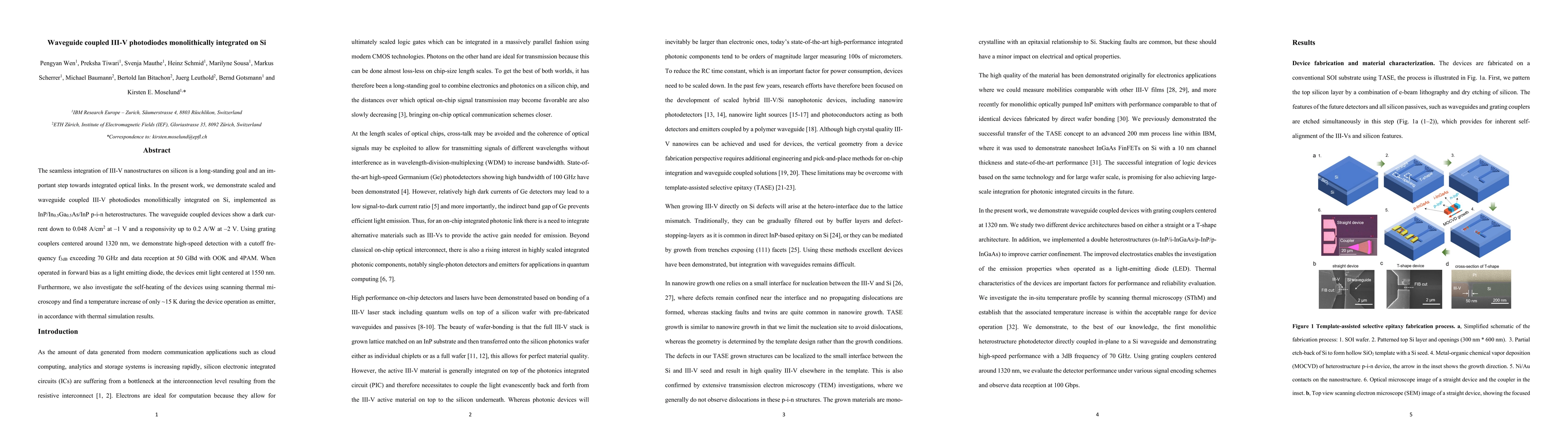
Abstract
The seamless integration of III-V nanostructures on silicon is a long-standing goal and an important step towards integrated optical links. In the present work, we demonstrate scaled and waveguide coupled III-V photodiodes monolithically integrated on Si, implemented as InP/In0.5Ga0.5As/InP p-i-n structure. The waveguide coupled devices show a dark current down to 0.048 A/cm2 at -1 V and a responsivity up to 0.2 A/W at -2 V. Using grating couplers centered around 1320 nm, we observed a cutoff frequency f3dB exceeding 70 GHz and data reception at 50 GBd with OOK and 4PAM. When operated in forward bias as light emitting diode, the devices emit light centered at 1550 nm. Furthermore, we also investigate the self-heating of the devices using scanning thermal microscopy and find a temperature increase of only ~15 K during the device operation as emitter, in accordance with thermal simulation results.
AI Key Findings
Get AI-generated insights about this paper's methodology, results, significance, and more — seven facets brought into focus.
Impact
Paper Details
Authors
PDF Preview
Key Terms
Citation Network
Current paper (gray), citations (green), references (blue)
Display is limited for performance on very large graphs.
Discussion 0