Publication
Metrics
AI Quick Summary
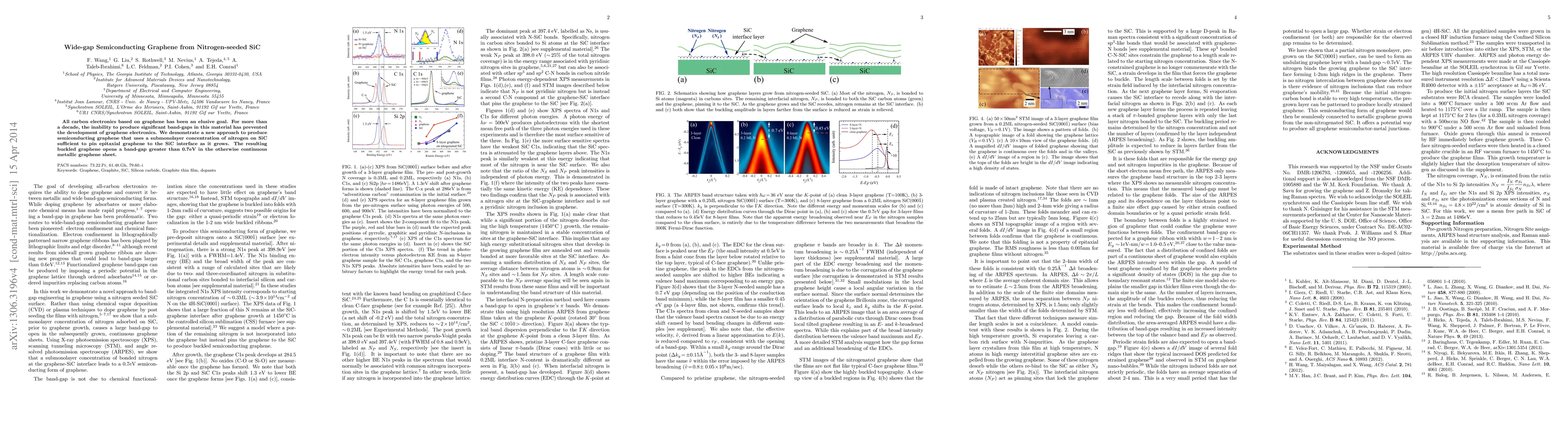
This paper presents a novel method to create wide-gap semiconducting graphene by using nitrogen-seeded silicon carbide (SiC) substrates. The approach involves pinning epitaxial graphene to the SiC interface with a submonolayer concentration of nitrogen, causing the graphene to buckle and open a band-gap greater than 0.7eV, overcoming the challenge of producing significant band-gaps in graphene.
Paper Preview
Abstract
All carbon electronics based on graphene has been an elusive goal. For more than a decade, the inability to produce significant band-gaps in this material has prevented the development of semiconducting graphene. While chemical functionalization was thought to be a route to semiconducting graphene, disorder in the chemical adsorbates, leading to low mobilities, have proved to be a hurdle in its production. We demonstrate a new approach to produce semiconducting graphene that uses a small concentration of covalently bonded surface nitrogen, not as a means to functionalize graphene, but instead as a way to constrain and bend graphene. We demonstrate that a submonolayer concentration of nitrogen on SiC is sufficient to pin epitaxial graphene to the SiC interface as it grows, causing the graphene to buckle. The resulting 3-dimensional modulation of the graphene opens a band-gap greater than 0.7eV in the otherwise continuous metallic graphene sheet.
AI Key Findings
Get AI-generated insights about this paper's methodology, results, significance, and more — seven facets brought into focus.
Impact
Paper Details
PDF Preview
Key Terms
Citation Network
Current paper (gray), citations (green), references (blue)
Display is limited for performance on very large graphs.
Discussion 0